ZHCSLE0B August 2021 – August 2023 JFE2140
PRODUCTION DATA
- 1
- 1 特性
- 2 应用
- 3 说明
- 4 Revision History
- 5 Pin Configuration and Functions
- 6 Specifications
- 7 Parameter Measurement Information
- 8 Detailed Description
- 9 Application and Implementation
- 10Device and Documentation Support
- 11Mechanical, Packaging, and Orderable Information
封装选项
机械数据 (封装 | 引脚)
散热焊盘机械数据 (封装 | 引脚)
- DSG|8
订购信息
7.1 AC Measurement Configurations
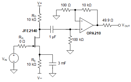
The circuit configuration used for noise measurements is seen in Figure 7-1. The nominal IDS current is configured in the schematic by calibrating V–. After IDS is fixed, the VDS voltage is set by calibrating V+. For input-referred noise data, the gain of the circuit is calibrated from VIN to VOUT and used for the input-referred gain calculation.
 Figure 7-1 AC Measurement Reference Schematic