SNVS082E December 2001 – May 2016 LM2593HV
PRODUCTION DATA.
- 1 Features
- 2 Applications
- 3 Description
- 4 Revision History
- 5 Pin Configuration and Functions
-
6 Specifications
- 6.1 Absolute Maximum Ratings
- 6.2 ESD Ratings
- 6.3 Recommended Operating Conditions
- 6.4 Thermal Information
- 6.5 Electrical Characteristics
- 6.6 Electrical Characteristics - 3.3-V Version
- 6.7 Electrical Characteristics - 5-V Version
- 6.8 Electrical Characteristics - Adjustable Voltage Version
- 6.9 Typical Characteristics
- 7 Parameter Measurement Information
- 8 Detailed Description
- 9 Application and Implementation
- 10Power Supply Recommendations
- 11Layout
- 12Device and Documentation Support
- 13Mechanical, Packaging, and Orderable Information
封装选项
机械数据 (封装 | 引脚)
散热焊盘机械数据 (封装 | 引脚)
- KTW|7
订购信息
7 Parameter Measurement Information
7.1 Test Circuits

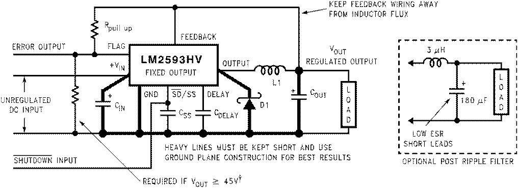
Component Values shown are for VIN = 15 V,
VOUT = 5 V, ILOAD = 2 A.
CIN — 470-µF, 50-V aluminum electrolytic Nichicon PM Series
COUT — 220-µF, 25-V aluminum electrolytic Nichcon PM Series
D1 — 3.3-A, 60-V Schottky Rectifier, 21DQ06 (international rectifier)
L1 — 33 µH, see Inductors Selection Procedure
Figure 23. Fixed Output Voltage Versions
VOUT = 5 V, ILOAD = 2 A.
CIN — 470-µF, 50-V aluminum electrolytic Nichicon PM Series
COUT — 220-µF, 25-V aluminum electrolytic Nichcon PM Series
D1 — 3.3-A, 60-V Schottky Rectifier, 21DQ06 (international rectifier)
L1 — 33 µH, see Inductors Selection Procedure

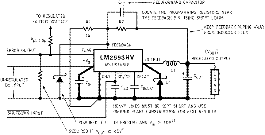
Select R1 to be approximately 1 kΩ, use a 1% resistor for best stability.
Component values shown are for VIN = 20 V,
VOUT = 10 V, ILOAD = 2 A.
CIN — 470-µF, 35-V aluminum electrolytic Nichicon PM Series
COUT — 220-µF, 35-V aluminum electrolytic Nichicon PM Series
D1 — 3.3-A, 60-V Schottky Rectifier, 21DQ06 (international rectifier)
L1 — 47 µH, see Inductors Selection Procedure
R1 — 1 kΩ, 1%
R2 — 7.15 k, 1%
CFF — 3.3 nF
Typical Values
CSS — 0.1 µF
CDELAY — 0.1 µF
RPULL UP — 4.7 k (use 22 k if VOUT is ≥ 45 V)
† Resistive divider is required to avoid exceeding maximum rating of 45 V, 3 mA on or into flag pin.
†† Small signal Schottky diode to prevent damage to feedback pin by negative spike when output is shorted (CFF not being able to discharge immediately will drag feedback pin below ground). Required if VIN > 40 V.
Figure 24. Adjustable Output Voltage Versions
Component values shown are for VIN = 20 V,
VOUT = 10 V, ILOAD = 2 A.
CIN — 470-µF, 35-V aluminum electrolytic Nichicon PM Series
COUT — 220-µF, 35-V aluminum electrolytic Nichicon PM Series
D1 — 3.3-A, 60-V Schottky Rectifier, 21DQ06 (international rectifier)
L1 — 47 µH, see Inductors Selection Procedure
R1 — 1 kΩ, 1%
R2 — 7.15 k, 1%
CFF — 3.3 nF
Typical Values
CSS — 0.1 µF
CDELAY — 0.1 µF
RPULL UP — 4.7 k (use 22 k if VOUT is ≥ 45 V)
† Resistive divider is required to avoid exceeding maximum rating of 45 V, 3 mA on or into flag pin.
†† Small signal Schottky diode to prevent damage to feedback pin by negative spike when output is shorted (CFF not being able to discharge immediately will drag feedback pin below ground). Required if VIN > 40 V.