ZHCSNW6G december 2003 – march 2023 LM2901-Q1 , LM2901AV-Q1 , LM2901B-Q1 , LM2901V-Q1
PRODMIX
- 1 特性
- 2 应用
- 3 说明
- 4 Revision History
- 5 Pin Configuration and Functions
-
6 Specifications
- 6.1 Absolute Maximum Ratings for LM2901B-Q1
- 6.2 Absolute Maximum Ratings for LM2901x-Q1
- 6.3 ESD Ratings for LM2901B-Q1
- 6.4 ESD Ratings for LM2901x-Q1
- 6.5 Recommended Operating Conditions for LM2901B-Q1
- 6.6 Recommended Operating Conditions for LM2901x-Q1
- 6.7 Thermal Information for LM2901B-Q1
- 6.8 Thermal Information for LM2901x-Q1
- 6.9 Electrical Characteristics for LM2901B-Q1
- 6.10 Switching Characteristics for LM2901B-Q1
- 6.11 Electrical Characteristics for LM2901x-Q1
- 6.12 Switching Characteristics for LM2901x-Q1
- 6.13 Typical Characteristics: LM2901B-Q1
- 6.14 Typical Characteristics: LM2901x-Q1
- 7 Detailed Description
- 8 Application and Implementation
- 9 Power Supply Recommendations
- 10Layout
- 11Device and Documentation Support
- 12Mechanical, Packaging, and Orderable Information
封装选项
请参考 PDF 数据表获取器件具体的封装图。
机械数据 (封装 | 引脚)
- D|14
- PW|14
- RTE|16
散热焊盘机械数据 (封装 | 引脚)
- RTE|16
订购信息
5 Pin Configuration and Functions
 Figure 5-1 D, PW and DYY Packages
14-Pin SOIC, TSSOP and SOT-23
Top View
 Figure 5-3 RUC Package
14-Pad X2QFN
Top View

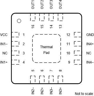
NOTE: Connect
exposed thermal pad directly to GND pin.
Figure 5-2 RTE Package16-Pad WQFN With Exposed Thermal Pad
Top View
Table 5-1 Pin Functions
| PIN | I/O | DESCRIPTION | |||
|---|---|---|---|---|---|
| NAME(1) | SOIC, TSSOP, DYY |
X2QFN | WQFN | ||
| OUT1 (1) | 1 | 14 | 16 | Output | Output pin of the comparator 2 |
| OUT2 (1) | 2 | 1 | 15 | Output | Output pin of the comparator 1 |
| VCC | 3 | 2 | 1 | — | Positive supply |
| IN2– (1) | 4 | 3 | 5 | Input | Negative input pin of the comparator 1 |
| IN2+ (1) | 5 | 4 | 6 | Input | Positive input pin of the comparator 1 |
| IN1– (1) | 6 | 5 | 2 | Input | Negative input pin of the comparator 2 |
| IN1+ (1) | 7 | 6 | 4 | Input | Positive input pin of the comparator 2 |
| IN3– | 8 | 7 | 7 | Input | Negative input pin of the comparator 3 |
| IN3+ | 9 | 8 | 8 | Input | Positive input pin of the comparator 3 |
| IN4– | 10 | 9 | 9 | Input | Negative input pin of the comparator 4 |
| IN4+ | 11 | 10 | 11 | Input | Positive input pin of the comparator 4 |
| GND | 12 | 11 | 12 | — | Negative supply |
| OUT4 | 13 | 12 | 13 | Output | Output pin of the comparator 4 |
| OUT3 | 14 | 13 | 14 | Output | Output pin of the comparator 3 |
| NC | — | — | 3 | — | No Internal Connection - Leave floating or GND |
| NC | — | — | 10 | — | No Internal Connection - Leave floating or GND |
| Thermal Pad | — | — | PAD | — | Connect directly to GND pin |
(1) Some manufacturers transpose the names of channels 1 & 2. Electrically the pinouts are identical, just a difference in channel naming convention.