SNVS443C May 2006 – December 2016 LM3489 , LM3489-Q1
PRODUCTION DATA.
- 1 Features
- 2 Applications
- 3 Description
- 4 Revision History
- 5 Pin Configuration and Functions
- 6 Specifications
- 7 Detailed Description
- 8 Application and Implementation
- 9 Power Supply Recommendations
- 10Layout
- 11Device and Documentation Support
- 12Mechanical, Packaging, and Orderable Information
7 Detailed Description
7.1 Overview
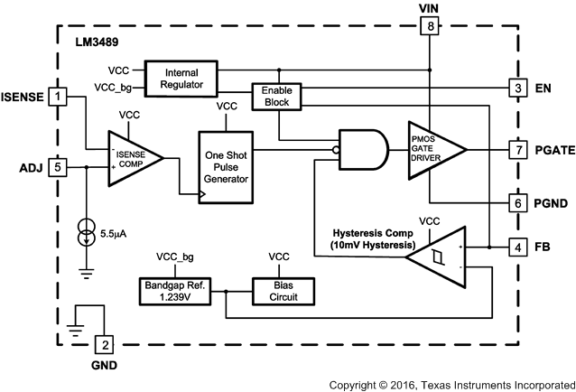
The LM3489 is a buck (step-down) DC-DC controller that uses a hysteretic control scheme. The control comparator is designed with approximately 10 mV of hysteresis. In response to the voltage at the FB pin, the gate drive (PGATE pin) turns the external PFET on or off. When the inductor current is too high, the current limit protection circuit engages and turns the PFET off for approximately 9 µs.
Hysteretic control does not require an internal oscillator. Switching frequency depends on the external components and operating conditions. The operating frequency reduces at light loads resulting in excellent efficiency compared to other architectures.
The output voltage can be programmed by two external resistors. The output can be set in a wide range from 1.239 V (typical) to VIN.
7.2 Functional Block Diagram
7.3 Feature Description
7.3.1 Hysteretic Control Circuit
When the FB input to the control comparator falls below the reference voltage (1.239 V), the output of the comparator switches to a low state. This results in the driver output, PGATE, pulling the gate of the PFET low and turning on the PFET. With the PFET on, the input supply charges COUT and supplies current to the load through the series path through the PFET and the inductor. Current through the Inductor ramps up linearly and the output voltage increases. As the FB voltage reaches the upper threshold, which is the internal reference voltage plus 10 mV, the output of the comparator changes from low to high, and the PGATE responds by turning the PFET off. As the PFET turns off, the inductor voltage reverses, the catch diode turns on, and the current through the inductor ramps down. Then, as the output voltage reaches the internal reference voltage again, the next cycle starts.
The LM3489 operates in discontinuous conduction mode at light-load current or continuous conduction mode at heavy-load current. In discontinuous conduction mode, current through the inductor starts at zero and ramps up to the peak then ramps down to zero. The next cycle starts when the FB voltage reaches the reference voltage. Until then, the inductor current remains zero and the output capacitor supplies the load. The operating frequency is lower and switching losses reduced. In continuous conduction mode, current always flows through the inductor and never ramps down to zero.
The output voltage (VOUT) can be programmed by 2 external resistors. It can be calculated with Equation 1.
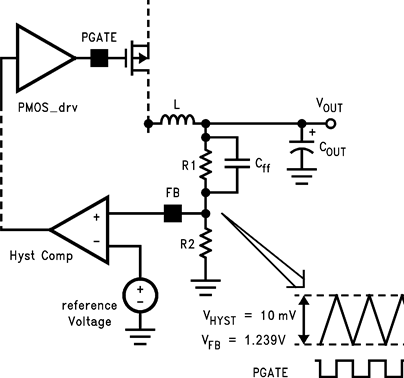 Figure 19. Hysteretic Window
The minimum output voltage ripple (VOUT_PP) can be calculated in the same way with Equation 2.
For example, with VOUT set to 3.3 V, VOUT_PP is 26.6 mV in Equation 3.
Operating frequency (F) is determined by knowing the input voltage, output voltage, inductor, VHYST, ESR (Equivalent Series Resistance) of output capacitor, and the delay. It can be approximately calculated using Equation 4.

where
- α: (R1 + R2) / R2
7.3.1.1 Delay
It includes the LM3489 propagation delay time and the PFET delay time. The propagation delay is 90 ns typically (see Figure 20).
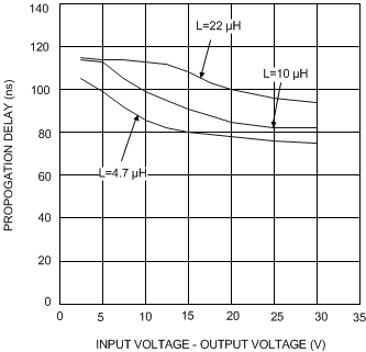 Figure 20. Propagation Delay
The operating frequency and output ripple voltage can also be significantly influenced by the speed up capacitor (Cff). Cff is connected in parallel with the high side feedback resistor, R1. The location of this capacitor is similar to where a phase lead capacitor would be located in a PWM control scheme. However it's effect on hysteretic operation is much different. Cff effectively shorts out R1 at the switching frequency and applies the full output ripple to the FB pin without dividing by the R2/R1 ratio. The end result is a reduction in output ripple and an increase in operating frequency. When adding Cff, calculate the formula above with α = 1. The value of Cff depend on the desired operating frequency and the value of R2. A good starting point is 470-pF ceramic at 100-kHz decreasing linearly with increased operating frequency. Also note that as the output voltage is programmed below 2.5 V, the effect of Cff will decrease significantly.
7.3.2 Current Limit Operation
The LM3489 has a cycle-by-cycle current limit. Current limit is sensed across the VDS of the PFET or across an additional sense resistor. When current limit is activated, the LM3489 turns off the external PFET for a period of 9 µs (typical). The current limit is adjusted by an external resistor, RADJ.
The current limit circuit is composed of the ISENSE comparator and the one-shot pulse generator. The positive input of the ISENSE comparator is the ADJ pin. An internal 5.5-µA current sink creates a voltage across the external RADJ resistor. This voltage is compared to the voltage across the PFET or sense resistor. The ADJ voltage can be calculated with Equation 5.
where
- 3 µA is the minimum ICL-ADJ value
The negative input of the ISENSE comparator is the ISENSE pin that must be connected to the drain of the external PFET. The inductor current is determined by sensing the VDS. It can be calculated with Equation 6.
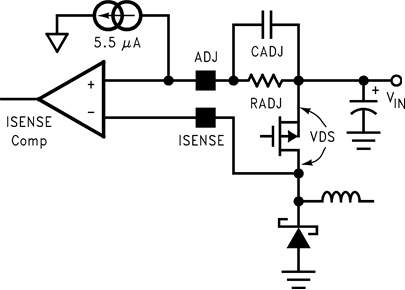 Figure 21. Current Sensing by VDS
The current limit is activated when the voltage at the ADJ pin exceeds the voltage at the ISENSE pin. The ISENSE comparator triggers the 9-µs one-shot pulse generator forcing the driver to turn the PFET off. The driver turns the PFET back on after 9 µs. If the current has not reduced below the set threshold, the cycle will repeat continuously.
A filter capacitor, CADJ, must be placed as shown in Figure 21. CADJ filters unwanted noise so that the ISENSE comparator will not be accidentally triggered. A value of 100 pF to 1 nF is recommended in most applications. Higher values can be used to create a soft-start function (see Start Up).
The current limit comparator has approximately 100 ns of blanking time. This ensures that the PFET is fully on when the current is sensed. However, under extreme conditions such as cold temperature, some PFETs may not fully turn on within the blanking time. In this case, the current limit threshold must be increased. If the current limit function is used, the on time must be greater than 100 ns. Under low duty cycle operation, the maximum operating frequency is limited by this minimum on-time.
During current limit operation, the output voltage drops significantly as does operating frequency. As the load current is reduced, the output returns to the programmed voltage. However, there is a current limit foldback phenomenon inherent in this current limit architecture (see Figure 22).
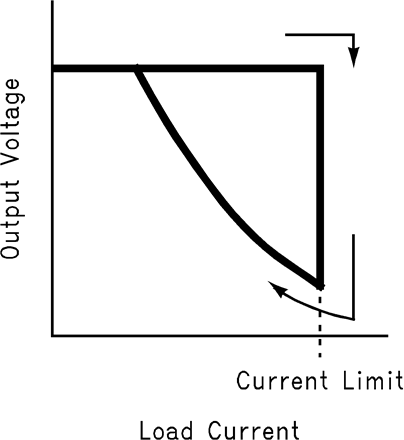 Figure 22. Current Limit Foldback Phenomenon
At high input voltages (> 28 V) increased undershoot at the switch node can cause an increase in the current limit threshold. To avoid this problem, a low Vf Schottky catch diode must be used (see Catch Diode Selection (D1)). Additionally, a resistor can be placed between the ISENSE pin and the switch node. Any value in the range of 220 Ω to 600 Ω is recommended.
7.3.3 Start Up
The current limit circuit is active during start-up. During start-up, the PFET stays on until either the current limit or the feedback comparator is tripped
If the current limit comparator is tripped first, then take the the foldback characteristic into account. Start-up into full load may require a higher current limit set point or the load must be applied after start-up.
One problem with selecting a higher current limit is inrush current during start-up. Increasing the capacitance (CADJ) in parallel with RADJ results in a soft-start characteristic. CADJ and RADJ create an RC time constant forcing current limit to activate at a lower current. The output voltage will ramp more slowly when using this technique. There is example start-up plot for CADJ equal to 1 nF in Typical Characteristics. Lower values for CADJ will have little to no effect on soft-start.
7.3.4 External Sense Resistor
The VDS of a PFET tends to vary significantly over temperature. This will result an equivalent variation in current limit. To improve current limit accuracy, an external sense resistor can be connected from VIN to the source of the PFET, as shown in Figure 23. The current sense resistor, RCS must have value comparable with RDSON of the PFET used, typically in the range of 50 mΩ to 200 mΩ. Equation 6 in Current Limit Operation can be used by replacing the RDSON with RCS.
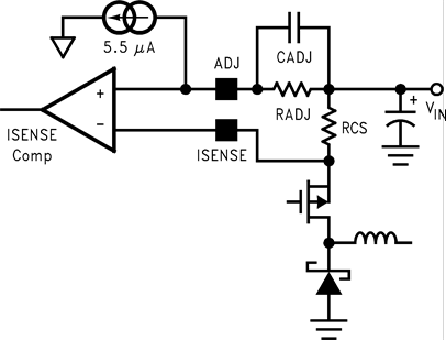 Figure 23. Current Sensing by External Resistor
7.3.5 PGATE
When switching, the PGATE pin swings from VIN (off) to some voltage below VIN (on). How far the PGATE will swing depends on several factors including the capacitance, on-time, and input voltage.
PGATE voltage swing will increase with decreasing gate capacitance. Although PGATE voltage will typically be around VIN-5V, with very small gate capacitances, this value can increase to a typical maximum of VIN-8.3 V.
Additionally, PGATE swing voltage will increase as on-time increases. During long on-times, such as when operating at 100% duty cycle, the PGATE voltage will eventually fall to its maximum voltage of VIN-8.3 V (typical) regardless of the PFET gate capacitance.
The PGATE voltage will not fall below 0.4 V (typical). Therefore, when the input voltage falls below approximately 9 V, the PGATE swing voltage range is reduced. At an input voltage of 7 V, for instance, PGATE will swing from 7 V to a minimum of 0.4 V.
7.3.6 Adjustable UVLO
The undervoltage lockout (UVLO) function can be implemented as shown in Figure 24. By incorporating the feature of the internal enable threshold, the lockout level can be programmed through an external potential divider formed with R3 and R4. The input voltage information is detected and compared with the enable threshold and the device operation is inhibited when VIN drops below the preset UVLO level. The UVLO and hysteresis voltage can be calculated with Equation 7 and Equation 8.


where
- VEN is the enable rising threshold voltage
- VEN_HYST is the enable threshold hysteresis
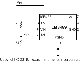 Figure 24. Adjustable UVLO
7.4 Device Functional Mode
7.4.1 Device Enable and Shutdown
The LM3489 can be remotely shutdown by forcing the enable pin to ground. With EN pin grounded, the internal blocks other than the enable logic are deactivated and the shutdown current of the device is lowered to only 7 µA (typical). Releasing the EN pin allows for normal operation to resume. The EN pin is internally pulled high with the voltage clamped at 8 V typical. For normal operation, this pin must be left open. In case an external voltage source is applied to this pin for enable control, the applied voltage must not exceed the maximum operating voltage level specified in this datasheet (that is 5.5 V).