SNVS569C May 2009 – October 2016 LM3550
PRODUCTION DATA.
- 1 Features
- 2 Applications
- 3 Description
- 4 Revision History
- 5 Pin Configuration and Functions
- 6 Specifications
-
7 Detailed Description
- 7.1 Overview
- 7.2 Functional Block Diagram
- 7.3 Feature Description
- 7.4 Device Functional Modes
- 7.5 Programming
- 7.6 Register Maps
- 8 Application and Implementation
- 9 Power Supply Recommendations
- 10Layout
- 11Device and Documentation Support
- 12Mechanical, Packaging, and Orderable Information
7 Detailed Description
7.1 Overview
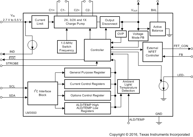
The LM3550 is a super-capacitor charger and high-current-flash controller based upon a switched-capacitor boost converter. On the charging end of the application, the LM3550 has a 534 mA (typical) input current limit that prevents the part from drawing an excessive current when the super-capacitor voltage is below the target charge voltage. During the charge phase the LM3550 runs in current limit and adaptively change gains (1×, 1.5×, 2×) until the super-capacitor reaches its target charge voltage. Integrated into the LM3550 is an external NFET controller that allows the flash current drawn from the super-capacitor to remain regulated throughout the flash cycle. Flash timing and current level can be changed through the I2C-compatible interface.
7.2 Functional Block Diagram
7.3 Feature Description
7.3.1 STROBE Pin
The STROBE pin on the LM3550 provides an external method of flash triggering. This means a direct connection between a controller or camera/imager and the LM3550 device can be made, avoiding any latency added due to communication delays. The STROBE pin can be configured to be rising-edge sensitive (default) or level sensitive. In the rising-edge sensitive mode, the flash duration is controlled internally and uses the value stored in the FLASH duration bits (Options Control Register bits 3:0) to determine the pulse length. If level sensitive mode is selected (Options Control Register bit 7 = 1), the flash-pulse duration can be controlled externally. In this mode, when the STROBE pin is high, the flash remains on as long as the duration does not exceed the value stored in the FLASH duration control bits. If the timing does exceed the internal flash-duration value, the LM3550 automatically disables the flash current.
7.3.2 End-of-Charge Pin (EOC)
The EOC pin provides an external flag alerting the microcontroller/microprocessor that the super-capacitor has reached the end of charging. When the super-capacitor has reached the desired end-of-charge level, the EOC pin transitions from its default state (logic 1) to the EOC state (logic 0). The EOC pin utilizes an open-drain driver that allows the EOC logic levels to be compatible with many of the common controller input/output (I/O) levels. Connecting a resistor between the system I/O supply and the EOC pin on the LM3550 ensures the proper voltage levels are utilized.
The state of the EOC pin can change during a flash event, or any other event whenever the super-capacitor voltage drops below 95% of the target charge voltage.
7.3.3 ALD/TEMP Pin
The ALD/TEMP pin allows the LM3550 to monitor the ambient light or ambient temperature and adjust the flash current through the LED/LEDs without requiring the microcontroller/microprocessor to issue commands through the control interface.
For ambient light detection, a reverse-biased photosensor/diode and a resistor are required. For ambient temperature sensing, a negative temperature coefficient (NTC) thermistor and a resistor are required. Internal to the LM3550 are two comparators (based on a 1-V reference) connected to the ALD/TEMP pin that provide three user-selectable regions of flash current adjustment. The trip-point thresholds are selectable in the ALD/TEMP Sense High and Low Registers.
If the ambient light or ambient temperature are sufficiently low (LM3550 in low region) the full-scale flash current is allowed. As the lighting conditions or temperature increase, the LM3550 ALD/TEMP detection circuit transitions to the second level that limits the flash current to 70% or the full-scale value. For conditions where a flash is not required (ambient detection) or if the ambient temperature is too high to flash safely, placing the ALD/TEMP circuit in the high-detection level, the LM3550 prevents a flash event from occurring. The functionality of the ALD/TEMP pin can be enabled or disabled through General Purpose Register (bit 6). These macro-functions, when enabled, off-load the microcontroller/microprocessor and provide significant system-power savings.
To help filter out the 50 to 60 Hz noise caused by indoor lighting, TI recommends a 1-µF ceramic capacitor tied between the ALD/TEMP pin and GND.
7.3.4 IND Pin
The Indicator pin (IND) consists of a current source that is capable of driving a red indicator LED with 5 mA of drive current. This indicator LED can be turned on and off by toggling bit 7 in the General Purpose Register.
7.3.5 BAL Pin
The Balance pin (BAL), when connected to a super-capacitor (if needed), regulates the two sections of the super-capacitor so that voltage on either cell is equal to ½ the output voltage. This ensures that an overvoltage condition on either capacitor section does not occur.
7.3.6 Super-Capacitor Charging Time
The time it takes the LM3550 to charge a super-capacitor from 0 V to the target voltage is highly dependent on the input voltage, output-voltage target, and super-capacitor capacitance value.
- The LM3550 up a capacitor faster if the target output voltage is lower and slower if the target output voltage is higher. For a given charge profile, a up a capacitor faster with higher input voltage and slower with lower input voltages. This is due to the LM3550 staying in the lower gains for longer periods of time.
- The LM3550 charges up a capacitor faster if the target output voltage is lower and slower if the target output voltage is higher. For a given charge profile, a lower capacitor voltage is reached faster than a higher voltage level.
- The LM3550 charges up a capacitor having a lower capacitance value faster than a capacitor having a higher capacitance level.
Table 1. Super-Capacitor Charging Times 0.5-F Capacitor, 0 V To Target
| OPTIMAL MODE(1) |
FIXED VOLTAGE MODE | |||
|---|---|---|---|---|
| VIN | 4.38 V | 4.5 V | 5 V | 5.3 V |
| 4.2 V | 4.565 s | 5.087 s | 6.314 s | 7.014 s |
| 3.6 V | 5.207 s | 5.765 s | 6.978 s | 7.832 s |
| 3 V | 6.090 s | 6.446 s | 7.870 s | 8.904 s |
7.3.7 Super-Capacitor Voltage Profile
When a constant load current is drawn from the charged super-capacitor, the voltage on the capacitor changes. The capacitor ESR and capacitance both affect the discharge profile.
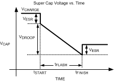
At the beginning of the flash (tSTART), the super-capacitor voltage drops due to the ESR of the super-capacitor. The magnitude of the drop is equal to the flash current (IFLASH) multiplied by the ESR (RESR).
Once the initial voltage drop occurs (VESR) the super-capacitor voltage decays at a constant rate until the flash ends (tFINISH). The voltage droop (VDROOP) during the flash event is equal to flash current (IFLASH) multiplied by the flash duration (tFLASH) divided by the capacitance value of the super-capacitor (CSC).
After the flash event has finished, the voltage on the super-capacitor increases due to the absence of current flowing through the ESR of the super-capacitor. This step-up is equal to
7.3.8 Peak Flash Current
To set the peak flash current controlled by the LM3550, a current setting resistor must be placed between the source of the current source and ground (FB to GND). The LM3550 regulates the voltage across the resistor to a value between 100 mV and 30 mV depending on the setting in the Current Control Register. Using the 100 mV setting, the peak flash current can be found usingEquation 4:
The LM3550 provides eight feedback voltage levels allowing eight different current settings. The current ranges from 100% of full-scale (100 mV setting) down to 30% of full-scale (30 mV setting) in 10% steps.
7.3.9 Maximum Flash Duration
Several factors determine the maximum achievable flash pulse duration. The flash current magnitude, feedback voltage, RDSON of the current source FET, super-capacitor capacitance (CSC), super-capacitor ESR (RESR) and super-capacitor charge voltage (VCAP) determine the ability of the device to regulate the flash current for a given amount of time.
where
- VDROOP = VCAP − VLED − [IFLASH × (RESR + RDSON + {RBAL/N)}] − VFB
- N = number of flash LEDs
Example:
If VCAP = 5.3 V, VLED = 4 V (at 1.5 A), IFLASH (total) = 3 A, CSC = 0.5 F, RESR = 50 mΩ, RDSON = 40 mΩ,
VFB = 100 mV, and RBAL = 75 mΩ, then VDROOP = 0.82 V and tFLASH (maximum) = 136 ms.
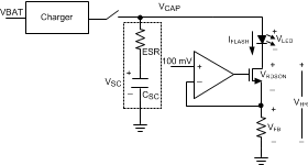 Figure 37. Power Loss Model
7.4 Device Functional Modes
7.4.1 State Machine Description
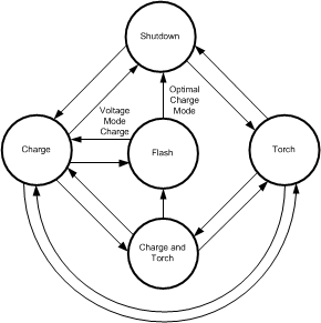 Figure 38. Default State Diagram
7.4.1.1 Basic Description
The state machine for the LM3550 involves five different states: shutdown, torch, charge, charge and torch, and flash.
The shutdown state, or standby state, places the LM3550 in a low-power mode that typically draws 1.8 µA of current from the power supply.
The torch state charges the super-capacitor up to VLED + VTREG (VTREG ≈ 300 mV) and utilizes the internal current sink to drive the flash LEDs with a current up to 200 mA.
The charge state places the LM3550 into a dedicated charge mode that provides the fastest means of charging the super-capacitor up to the target level (4.5 V, 5 V, 5.3 V or optimal).
The charge and torch state combines the functionality of both the torch state and charge state. This state allows the flash LEDs to be on during the charging of the super-capacitor. During the initial charging, the torch current is limited to 60 mA to allow the majority of the output current to be utilized in the super-capacitor charging. Once the target capacitor voltage is reached, the torch-current levels become fully adjustable.
The Flash state is responsible for driving the flash LEDs at the desired flash current. This state can be entered either through I2C-controlled event or through an external strobe event.
7.4.1.2 Shutdown State
The shutdown state is the default power-up state. The LM3550 enters the shutdown state when the STROBE pin is held low without a flash event occurring, and when the flash, torch, and charge bits in the General Purpose Register are equal to 0.
7.4.1.3 Torch State
The torch state of the LM3550 provides the flash LED / LEDs with a constant current level that is safe for continuous operation. This state is useful in low light conditions when an imager is placed in movie or video mode. The torch state is enabled when the torch bit in the General Purpose Register is set to a 1 and the flash and charge bits are set to 0. The desired torch current level (8 total levels between 60 mA and 200 mA) is set in the Current Control Register.
Enabling the torch bit starts up the LM3550 and begin charging the capacitor. Before a torch event can occur, the super-capacitor must be charged to a voltage greater than 3 V. Once the super-capacitor reaches a voltage of 3 V, the LED− pin begins sinking current. In order for the torch current to be properly regulated, the super-capacitor must be charged up to a value that is greater than VLED + VTREG (VTREG ≈ 300 mV).
When in the torch state, the LM3550 regulates the proper output voltage (either 3 V or VLED + VREG) utilizing a pulsed regulation scheme (PFM). During this mode, the device operate in current limit until the output voltage reaches the target level. At that point, the charge-pump turns off, and the super-capacitor supplies the load. Once the super-capacitor voltage drops below the turnon threshold due to the loading caused by the torch current, the charge-pump turns on again and re-charges the super-capacitor.
7.4.1.4 Charge State
The charge state of the LM3550 provides the fastest charge time when compared to the other states of operation. In this state, the user has the option of charging the super-capacitor to a voltage equal to 4.5 V, 5 V, 5.3 V or to an optimal voltage. The charge state is enabled through the I2C interface by setting the charge bit to a 1 and setting the flash and torch Bits to a 0 in the General Purpose Register. The charge voltage is selectable by setting the two charge-mode bits (CM1 and CM0) also found in the General Purpose Register.
Depending on the input voltage and output voltage conditions, the LM3550 delivers different charge currents to the super-capacitor. Charge current is dependent on the charge-pump gain.
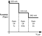 Figure 39. Charge Current vs Output Voltage
7.4.1.4.1 Fixed-Voltage-Charge Mode
During the charge state, the LM3550 operates in current limit until the target voltage is reached. For the 4.5 V, 5 V and 5.3 V charge modes, the LM3550 operates in a constant-frequency mode once the target voltage is reached for load currents greater than 60 mA. This allows the LM3550 to draw only the required current from the power source when the load current is less than the maximum. When the average output current exceeds the maximum of the LM3550, the device returns to the current limited operation until the target voltage is reached. If the output current is less than 60 mA, the LM3550 operates in a PFM-burst mode.
7.4.1.4.2 Optimal Charge Mode
For the optimal charge mode, the current-limited, pulsed-regulation scheme (PFM) is used to maintain the target voltage. In optimal charge mode, the LM3550 charges the super-capacitor to a level that is required to sustain a flash for a given period of time. optimal charge mode compensates for variations in LED forward voltage and super-capacitor ESR by charging the capacitor to an optimal voltage that minimizes the power dissipated in the external current source during the flash. The user must calculate the required overhead voltage and select this value in the Options Control Register. For more information regarding the optimal charge mode, see the Application and Implementation description.
NOTE
When the LM3550 is placed into optimal charge mode, the flash LEDs begin to glow once the super-capacitor voltage exceeds 3 V. The LEDs continue to glow until the device is placed into shutdown, into the flash state, or into one of the fixed-voltage charge modes.
7.4.1.5 Torch and Charge State
The torch and charge state provides the ability to utilize the torch functionality while charging to the selected target voltage. The torch and charge state is entered by setting the torch bit and charge bit to a 1 and by setting the flash bit to a 0 in the General Purpose Register. Additionally, the CM1 and CM0 bits can be configured to define the target charge voltage.
During the initial charging of the super-capacitor, the torch functionality is enabled until the capacitor voltage reaches 3 V. Additionally, the torch current is limited to 60 mA until the target voltage is reached. Once the output reaches the target, the current level specified in the Current Control Register is allowed.
In the event that the total output current exceeds the capacitor charge current (ICHARGE = IMAX − ITORCH − IEXTERNAL), causing the super-capacitor to drop below the target voltage, the LM3550 automatically sets the T2 bit in the Current Control Register to a 0, decreasing the torch current.
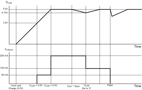 Figure 40. Torch Current Diagram
7.4.1.6 Flash State
When entered, the flash state of the LM3550 device delivers a high-current burst of current to the flash LEDs. To enter the flash state, the flash bit in the General Purpose Register must be set to a 1 or the STROBE pin must be pulled high (edge or level sensitive). The flash duration and current level are user adjustable via the I2C interface (F2-F0 in current control and FD3-FD0 in options).
By default, a flash does not occur if the super-capacitor is not fully charged (that is, the end-of-charge flag (EOC pin) must transition low). If the flash state was entered via the I2C interface (flash bit = 1 ), the LM3550 automatically resets the flash bit and the torch bit to 0 upon completion of the flash. Additionally, after the flash event has occurred, the LM3550 returns to the charge state/mode that was in operation before the flash event with the exception of optimal charge mode. (If optimal charge mode was used before a flash, all charging is halted after the flash.)
7.4.1.7 EOC Functionality
The EOC pin of the device provides an indicator alerting the controller that the super-capacitor has reached its target voltage. The EOC pin transitions low once the capacitor reaches 95% of the target voltage for the 4.5 V, 5 V and 5.3 V modes or once the capacitor has reached the optimal charge voltage in optimal charge mode.
During operation, the LM3550 continues to monitor the voltage on the super-capacitor and updates the EOC pin when needed. Any time a mode transition occurs during charge mode or charge and torch mode, the EOC state is re-evaluated.
During torch mode, the EOC always indicates a charging state (EOC = 1) .
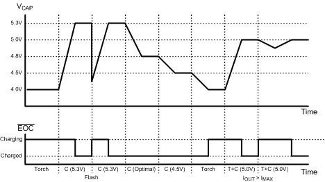
7.4.1.8 State Diagram FGATE = 1
By default, the LM3550 prevents a flash event from occurring if the super-capacitor has not reached the target voltage (EOC = 0). In the event that this restriction is not desired, the flash gate bit (FGATE in the General Purpose Register) can be set to a 1 disabling the end-of-charge requirement. Setting FGATE to a 1 allows the flash state to be entered at anytime. If the super-capacitor is not charged to the proper voltage before the EOC pin indicates a full charge, the perceived duration and flash level could be lower than desired.
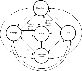 Figure 41. FGATE = 1 State Diagram
7.4.1.9 Optimal Charge Mode vs Fixed Voltage Mode
The LM3550 provides two types of super-capacitor charging modes: fixed voltage and optimal charge.
In fixed voltage mode, the LM3550 charges and regulate the super-capacitor to either 4.5 V, 5 V, or 5.3 V. This mode is useful if the LM3550 is going to be used for both flash and fixed-rail applications (power supply for audio or PA sub-systems).
If the LM3550 is only going to be used as a super-capacitor charger and flash controller, the optimal charge mode provides many advantages over the fixed voltage mode. optimal charge mode charges the super-capacitor to the minimum voltage that is required to sustain a flash pulse compensating for variations in super-capacitor ESR and LED forward voltage due to temperature and process. To properly use the optimal charge mode, the overhead voltage (VOH) must be determined. The overhead voltage is equal to the voltage required to maintain current source regulation (VHR) plus the voltage droop (VDROOP) on the super-capacitor due to the flash event.
and
where
- N = Number of flash LEDs
Example:
If VLED (peak)= 4.1 V (at 1.5 A), IFLASH (total) = 3 A, CSC = 0.5 F, RESR = 50 mΩ, RDSON = 40 mΩ, VFB = 100 mV, RBAL = 75 mΩ, and tFLASH = 64 ms, then VOH = 0.604 V and VCAP = 4.97 V.
NOTE
VLED (peak) is equal to the LED voltage before self-heating occurs. Once current flows through the LED, the LED heats up, and the forward voltage decreases until it reaches a steady-state level. This voltage drop is dependent on the LED and the PCB layout.
Based on this calculation, setting the overhead voltage to 600 mV in the Current Control Register should ensure a regulated 3-A flash pulse over the entire flash duration.
Unlike fixed voltage mode, optimal charge mode adjusts the super-capacitor voltage upon changes in LED forward voltage and variation in super-capacitor ESR, ensuring that the super-capacitor does not charge to a voltage higher than needed. By charging optimally, the LM3550 can potentially charge the super-capacitor to its EOC state faster due to the target voltage being lower, and it helps ease the thermal loading on the current source FET during the flash.
7.4.1.9.1 Optimal Charge Mode vs Fixed Voltage Mode
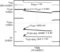 Figure 42. Optimal Charge Mode
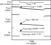 Figure 43. 5.3-V Fixed Voltage Charge Mode
Peak power dissipation across current source FET
where
- Optimal mode = 1.5 W, fixed voltage mode (5.3 V) = 2.4 W
Average power dissipation across current source FET (64 ms pulse)
where
- Optimal mode = 936 mW, fixed voltage mode (5.3 V) = 1.824 W
7.5 Programming
7.5.1 I2C-Compatible Interface
7.5.1.1 Data Validity
The data on SDA line must be stable during the HIGH period of the clock signal (SCL). In other words, the state of the data line can only be changed when SCL is LOW.
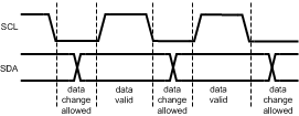 Figure 44. Data Validity Diagram
A pullup resistor between VIO (logic power supply) and SDA must be greater than [(VIO − VOL) / 3 mA] to meet the VOL requirement on SDA. Using a larger pullup resistor results in lower switching current with slower edges, while using a smaller pullup resistor results in higher switching currents with faster edges.
7.5.1.2 Start and Stop Conditions
START and STOP conditions classify the beginning and the end of the I2C session. A START condition is defined as SDA signal transitioning from HIGH to LOW while SCL line is HIGH. A STOP condition is defined as the SDA transitioning from LOW to HIGH while SCL is HIGH. The I2C master always generates START and STOP conditions. The I2C bus is considered to be busy after a START condition and free after a STOP condition. During data transmission, the I2C master can generate repeated START conditions. First START and repeated START conditions are equivalent, function-wise. The data on SDA line must be stable during the HIGH period of the clock signal (SCL). In other words, the state of the data line can only be changed when SCL is LOW.
 Figure 45. Start and Stop Conditions
7.5.1.3 Transferring Data
Every byte put on the SDA line must be eight bits long, with the most significant bit (MSB) being transferred first. Each byte of data has to be followed by an acknowledge bit. The acknowledge-related clock pulse is generated by the master. The master releases the SDA line (HIGH) during the acknowledge clock pulse. The LM3550 pulls down the SDA line during the 9th clock pulse, signifying an acknowledge. The LM3550 generates an acknowledge after each byte has been received.
After the START condition, the I2C master sends a chip address. This address is seven bits long followed by an eighth bit which is a data direction bit (R/W). The LM3550 address is 53h. For the eighth bit, a 0 indicates a WRITE and a 1 indicates a READ. The second byte selects the register to which the data will be written. The third byte contains data to write to the selected register.
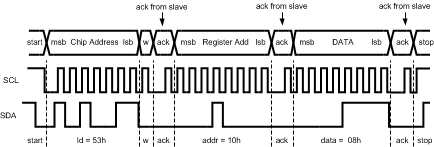
ack = acknowledge (SDA pulled down by the slave)
id = chip address, 53h for LM3550
7.5.1.4 I2C-Compatible Child Address: 0x53

7.6 Register Maps
7.6.1 Internal Registers
| Register | Internal Hex Address | Power On Value |
|---|---|---|
| General Purpose | 0x10 | 0000 0000 |
| Current Control | 0xA0 | 1111 1000 |
| Options | 0xB0 | 1000 0000 |
| ALD/TEMP Sense High | 0xC0 | 1111 1001 |
| ALD/TEMP Sense Low | 0xD0 | 1100 0110 |
7.6.1.1 General Purpose Register Description

FLASH, CHARGE, and TORCH: Mode Bits (see Table 2).
CM0–CM1: Capacitor Charge Mode (see Table 3).
FGATE: Flash Gate Bit. If FGATE is a 0, then an end-of-charge condition must occur before a flash can take place. If FGATE is a 1, then an end-of-charge condition does not have to occur before a flash can take place.
A/T EN: ALD/TEMP Enable Bit
IND EN: Enable Indicator Current Source (0 = Indicator Off, 1 = Indicator On)
Table 2. Control Modes
| Flash | Charge | Torch | Mode |
|---|---|---|---|
| 0 | 0 | 0 | Disabled |
| 0 | 0 | 1 | Torch |
| 0 | 1 | 0 | Charge |
| 0 | 1 | 1 | Charge and Torch |
| 1 | x | x | Flash |
Table 3. Capacitor Charge Level
| CM1 | CM0 | Level |
| 0 | 0 | Optimal Charge Mode |
| 0 | 1 | 4.5 |
| 1 | 0 | 5.0V |
| 1 | 1 | 5.3V |
Table 4. Gated Flash Control
| FGATE Bit | Result |
|---|---|
| 0 | Flash only allowed after EOC reached |
| 1 | Flash allowed without EOC reached |
Table 5. ALD/TEMP Control
| A/T EN Bit | Result |
|---|---|
| 0 | ALD MODE DISABLED |
| 1 | ALD MODE ENABLED |
7.6.1.2 Current Control Register Description

Table 6. Torch Level Table
| T2 | T1 | T0 | Level |
|---|---|---|---|
| 0 | 0 | 0 | 60 mA |
| 0 | 0 | 1 | 80 mA |
| 0 | 1 | 0 | 100 mA |
| 0 | 1 | 1 | 120 mA |
| 1 | 0 | 0 | 140 mA |
| 1 | 0 | 1 | 160 mA |
| 1 | 1 | 0 | 180 mA |
| 1 | 1 | 1 | 200 mA |
Table 7. Flash Level Table
| F2 | F1 | F0 | FB Voltage Level |
|---|---|---|---|
| 0 | 0 | 0 | 30 mV |
| 0 | 0 | 1 | 40 mV |
| 0 | 1 | 0 | 50 mV |
| 0 | 1 | 1 | 60 mV |
| 1 | 0 | 0 | 70 mV |
| 1 | 0 | 1 | 80 mV |
| 1 | 1 | 0 | 90 mV |
| 1 | 1 | 1 | 100 mV |
7.6.1.3 Options Control Register Description

SLE: Strobe Level or Edge Sensitivity. 0 = Edge Sensitive, 1 = Level Sensitive
FD0-FD3: Flash Duration control bits (see Table 8).
OH0-OH2: Overhead Charge Voltage control bits (see Table 9).
Table 8. Time-out Duration Table
| FD3 | FD2 | FD1 | FD0 | Time (msec) |
|---|---|---|---|---|
| 0 | 0 | 0 | 0 | 16 |
| 0 | 0 | 0 | 1 | 32 |
| 0 | 0 | 1 | 0 | 48 |
| 0 | 0 | 1 | 1 | 64 |
| 0 | 1 | 0 | 0 | 80 |
| 0 | 1 | 0 | 1 | 96 |
| 0 | 1 | 1 | 0 | 112 |
| 0 | 1 | 1 | 1 | 128 |
| 1 | 0 | 0 | 0 | 144 |
| 1 | 0 | 0 | 1 | 160 |
| 1 | 0 | 1 | 0 | 176 |
| 1 | 0 | 1 | 1 | 192 |
| 1 | 1 | 0 | 0 | 208 |
| 1 | 1 | 0 | 1 | 224 |
| 1 | 1 | 1 | 0 | 240 |
| 1 | 1 | 1 | 1 | 512 |
Table 9. Overhead Charge Voltage Table
| OH2 | OH1 | OH0 | Level |
|---|---|---|---|
| 0 | 0 | 0 | 300 mV |
| 0 | 0 | 1 | 400 mV |
| 0 | 1 | 0 | 500 mV |
| 0 | 1 | 1 | 600 mV |
| 1 | 0 | 0 | 700 mV |
| 1 | 0 | 1 | 800 mV |
| 1 | 1 | 0 | 900 mV |
| 1 | 1 | 1 | 1V |
7.6.1.4 ALD/TEMP Sense High/Low Registers
 Figure 47. ALD/TEMP Sense High Register
 Figure 48. ALD/TEMP Sense Low Register
For ALD/TEMP Sense High and ALD/TEMP sense low, the trip levels are set by Equation 10:
where
- N is the decimal equivalent of the value stored in the ALD/TEMP Sense High/Low registers
NSENSEHIGH must be greater than NSENSELOW.