ZHCSQD0 April   2022 LM5013-Q1

PRODUCTION DATA  

  1. 特性
  2. 应用
  3. 说明
  4. Revision History
  5. Pin Configuration and Functions
  6. Specifications
    1. 6.1 Absolute Maximum Ratings
    2. 6.2 ESD Ratings
    3. 6.3 Recommended Operating Conditions
    4. 6.4 Thermal Information
    5. 6.5 Electrical Characteristics
    6. 6.6 Typical Characteristics
  7. Detailed Description
    1. 7.1 Overview
    2. 7.2 Functional Block Diagram
    3. 7.3 Feature Description
      1. 7.3.1  Control Architecture
      2. 7.3.2  Internal VCC Regulator and Bootstrap Capacitor
      3. 7.3.3  Regulation Comparator
      4. 7.3.4  Internal Soft Start
      5. 7.3.5  On-Time Generator
      6. 7.3.6  Current Limit
      7. 7.3.7  N-Channel Buck Switch and Driver
      8. 7.3.8  Schottky Diode Selection
      9. 7.3.9  Enable/Undervoltage Lockout (EN/UVLO)
      10. 7.3.10 Power Good (PGOOD)
      11. 7.3.11 Thermal Protection
    4. 7.4 Device Functional Modes
      1. 7.4.1 Shutdown Mode
      2. 7.4.2 Standby Mode
      3. 7.4.3 Active Mode
      4. 7.4.4 Sleep Mode
  8. Application and Implementation
    1. 8.1 Application Information
    2. 8.2 Typical Application
      1. 8.2.1 Design Requirements
      2. 8.2.2 Detailed Design Procedure
        1. 8.2.2.1 Custom Design With WEBENCH® Tools
        2. 8.2.2.2 Switching Frequency (RRON)
        3. 8.2.2.3 Buck Inductor (LO)
        4. 8.2.2.4 Schottky Diode (DSW)
        5. 8.2.2.5 Output Capacitor (COUT)
        6. 8.2.2.6 Input Capacitor (CIN)
        7. 8.2.2.7 Type 3 Ripple Network
      3. 8.2.3 Application Curves
  9. Power Supply Recommendations
  10. 10Layout
    1. 10.1 Layout Guidelines
      1. 10.1.1 Compact PCB Layout for EMI Reduction
      2. 10.1.2 Feedback Resistors
    2. 10.2 Layout Example
      1. 10.2.1 Thermal Considerations
  11. 11Device and Documentation Support
    1. 11.1 Device Support
      1. 11.1.1 第三方米6体育平台手机版_好二三四免责声明
      2. 11.1.2 Development Support
        1. 11.1.2.1 Custom Design With WEBENCH® Tools
    2. 11.2 Documentation Support
      1. 11.2.1 Related Documentation
    3. 11.3 接收文档更新通知
    4. 11.4 支持资源
    5. 11.5 Trademarks
    6. 11.6 Electrostatic Discharge Caution
    7. 11.7 术语表
  12. 12Mechanical, Packaging, and Orderable Information

封装选项

机械数据 (封装 | 引脚)
散热焊盘机械数据 (封装 | 引脚)
订购信息

Layout Example

Figure 10-2 shows an example layout for the PCB top layer of a 2-layer board with essential components placed on the top side.
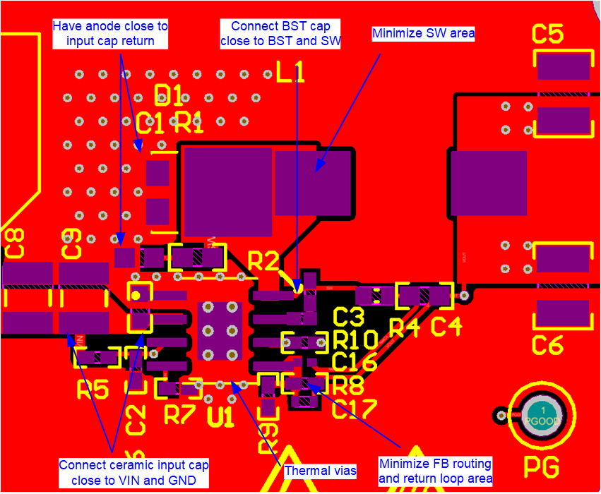
GUID-20211117-SS0I-KDBT-GC2N-7BHPLRM9M8H4-low.pngFigure 10-2 LM5013-Q1 Layout Example