ZHCSEV7I June 2011 – October 2019 LM5113
PRODUCTION DATA.
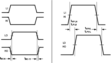
6.6 Switching Characteristics
over operating free-air temperature range (unless otherwise noted)| PARAMETER | TEST CONDITIONS | MIN | TYP | MAX | UNIT | ||
|---|---|---|---|---|---|---|---|
| tLPHL | LO turnoff propagation delay | LI falling to LOL falling | TJ = 25°C | 26.5 | ns | ||
| TJ = –40°C to 125°C | 45.0 | ||||||
| tLPLH | LO turnon propagation delay | LI rising to LOH rising | TJ = 25°C | 28.0 | ns | ||
| TJ = –40°C to 125°C | 45.0 | ||||||
| tHPHL | HO turnoff propagation delay | HI falling to HOL falling | TJ = 25°C | 26.5 | ns | ||
| TJ = –40°C to 125°C | 45.0 | ||||||
| tHPLH | HO turnon propagation delay | HI rising to HOH rising | TJ = 25°C | 28.0 | ns | ||
| TJ = –40°C to 125°C | 45.0 | ||||||
| tMON | Delay matching
LO on & HO off |
TJ = 25°C | 1.5 | ns | |||
| TJ = –40°C to 125°C | 8.0 | ||||||
| tMOFF | Delay matching
LO off & HO on |
TJ = 25°C | 1.5 | ns | |||
| TJ = –40°C to 125°C | 8.0 | ||||||
| tHRC | HO rise time (0.5 V – 4.5 V) | CL = 1000 pF | 7.0 | ns | |||
| tLRC | LO rise time (0.5 V – 4.5 V) | CL = 1000 pF | 7.0 | ns | |||
| tHFC | HO fall time (0.5 V – 4.5 V) | CL = 1000 pF | 1.5 | ns | |||
| tLFC | LO fall time (0.5 V – 4.5 V) | CL = 1000 pF | 1.5 | ns | |||
| tPW | Minimum input pulse width
that changes the output |
10 | ns | ||||
| tBS | Bootstrap diode
reverse recovery time |
IF = 100 mA, IR = 100 mA | 40 | ns | |||
(1) Minimum and maximum limits are 100% production tested at 25°C. Limits over the operating temperature range are ensured through correlation using Statistical Quality Control (SQC) methods. Limits are used to calculate Average Outgoing Quality Level (AOQL).
 Figure 1. Timing Diagram