ZHCSEV7I June 2011 – October 2019 LM5113
PRODUCTION DATA.
6.7 Typical Characteristics
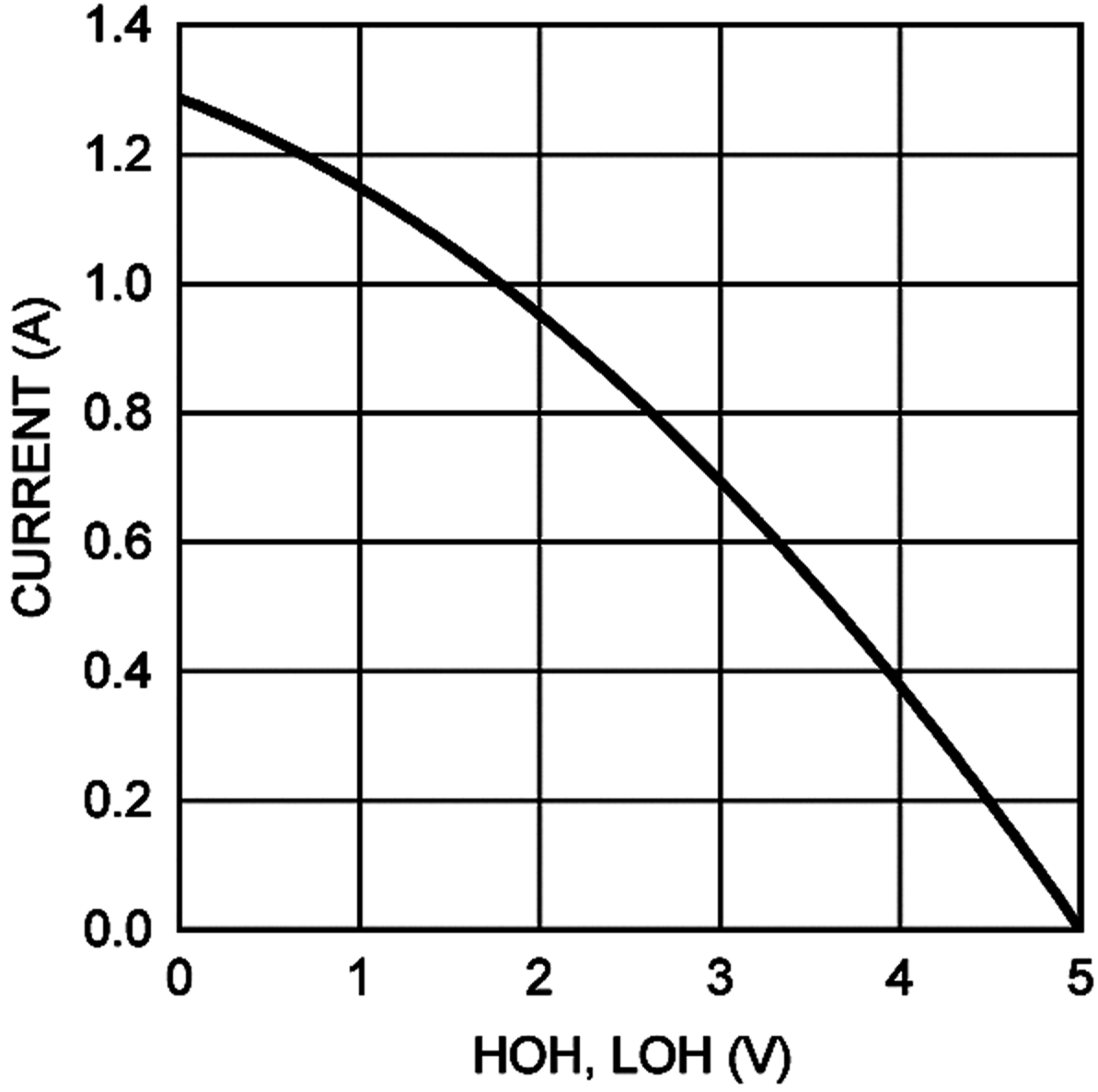 Figure 2. Peak Source Current vs Output Voltage
 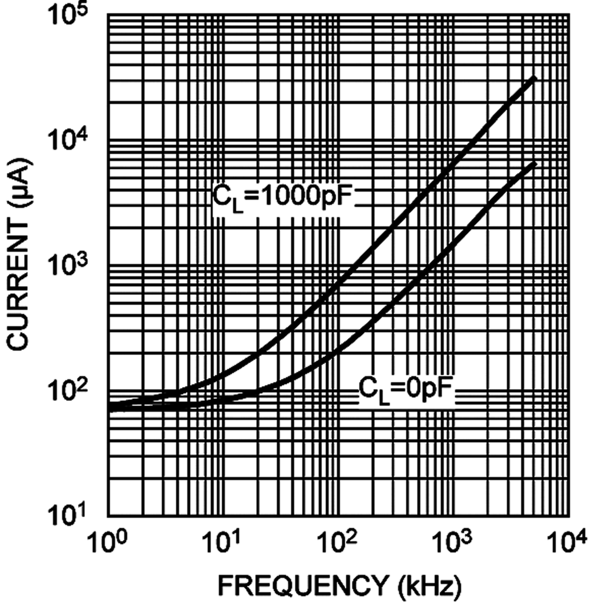 Figure 4. IDDO vs Frequency
 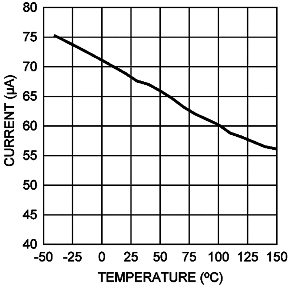 Figure 6. IDD vs Temperature
 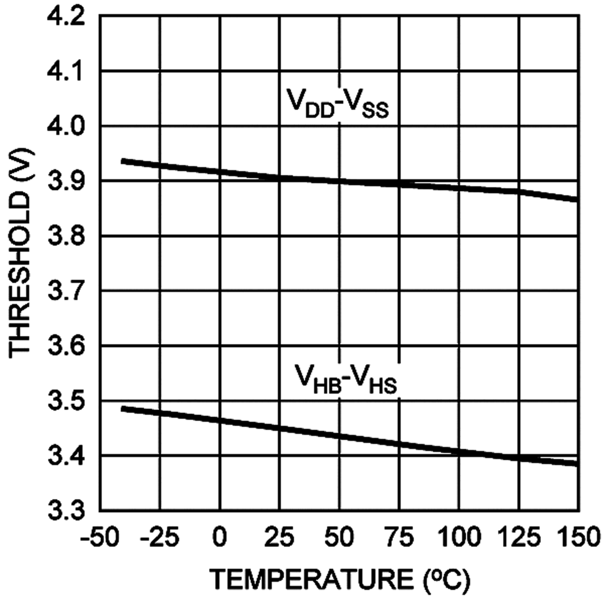 Figure 8. UVLO Rising Thresholds vs Temperature
 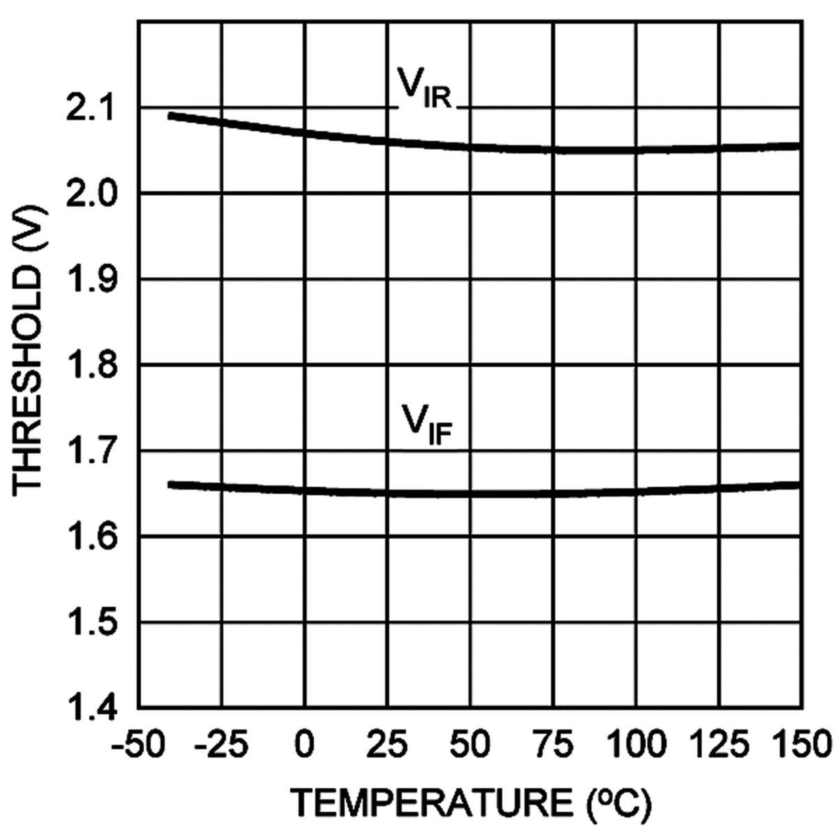 Figure 10. Input Thresholds vs Temperature
 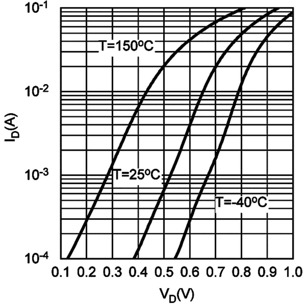 Figure 12. Bootstrap Diode Forward Voltage
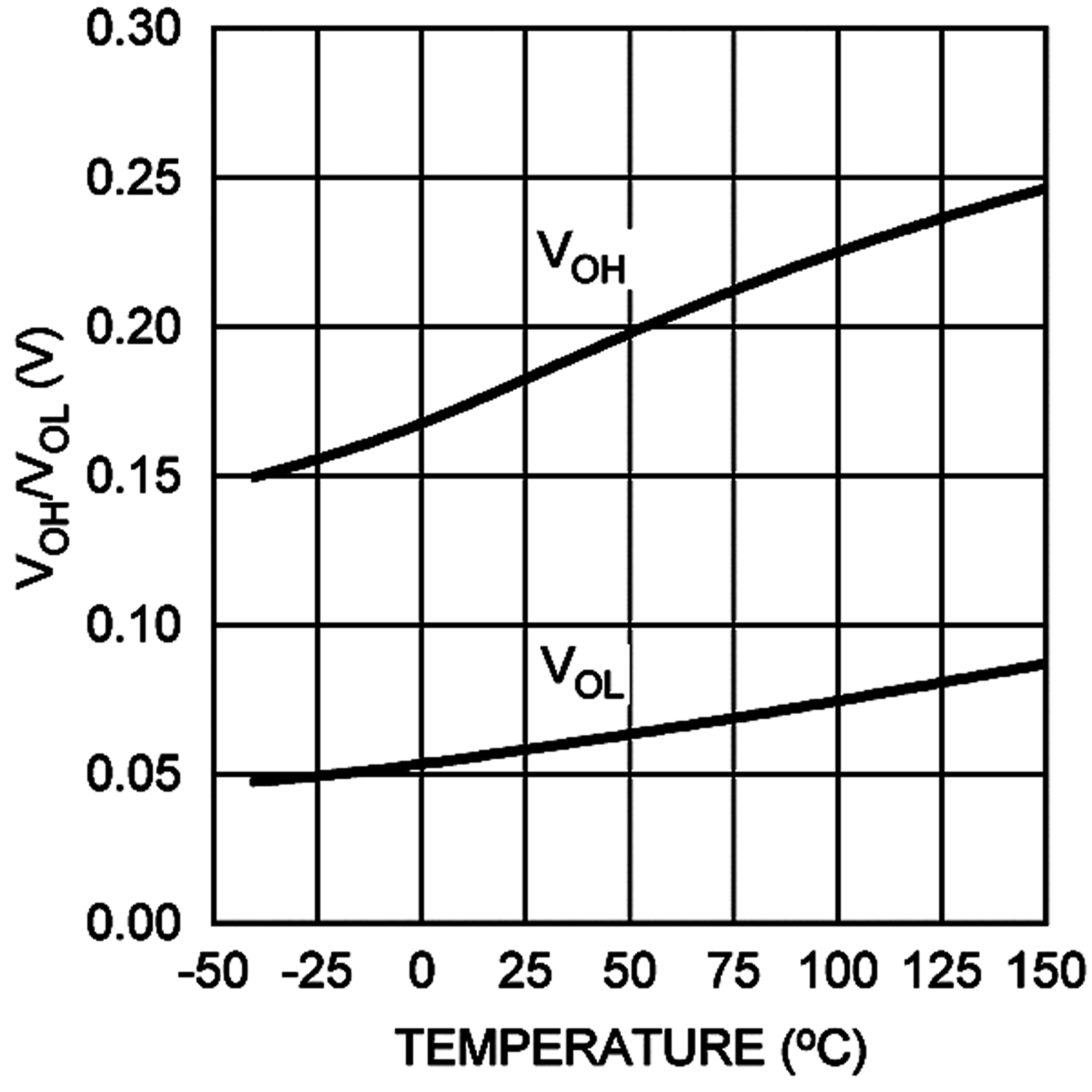
| Note: Unless otherwise specified, | ||
| VDD = VHB = 5 V, VSS = VHS = 0 V. | ||
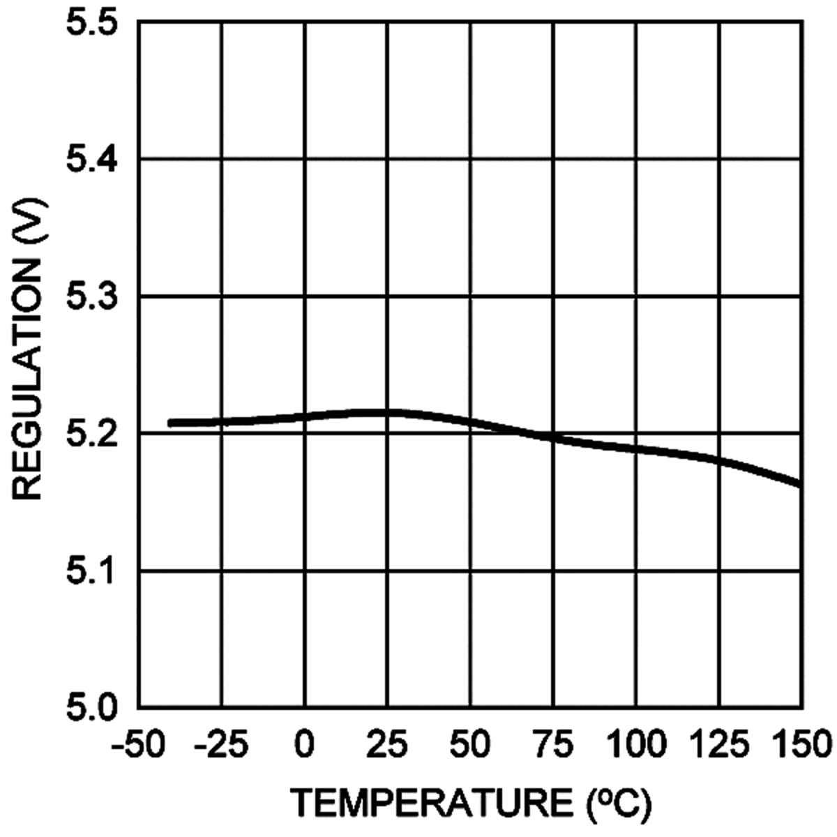
Output Voltage vs Temperature
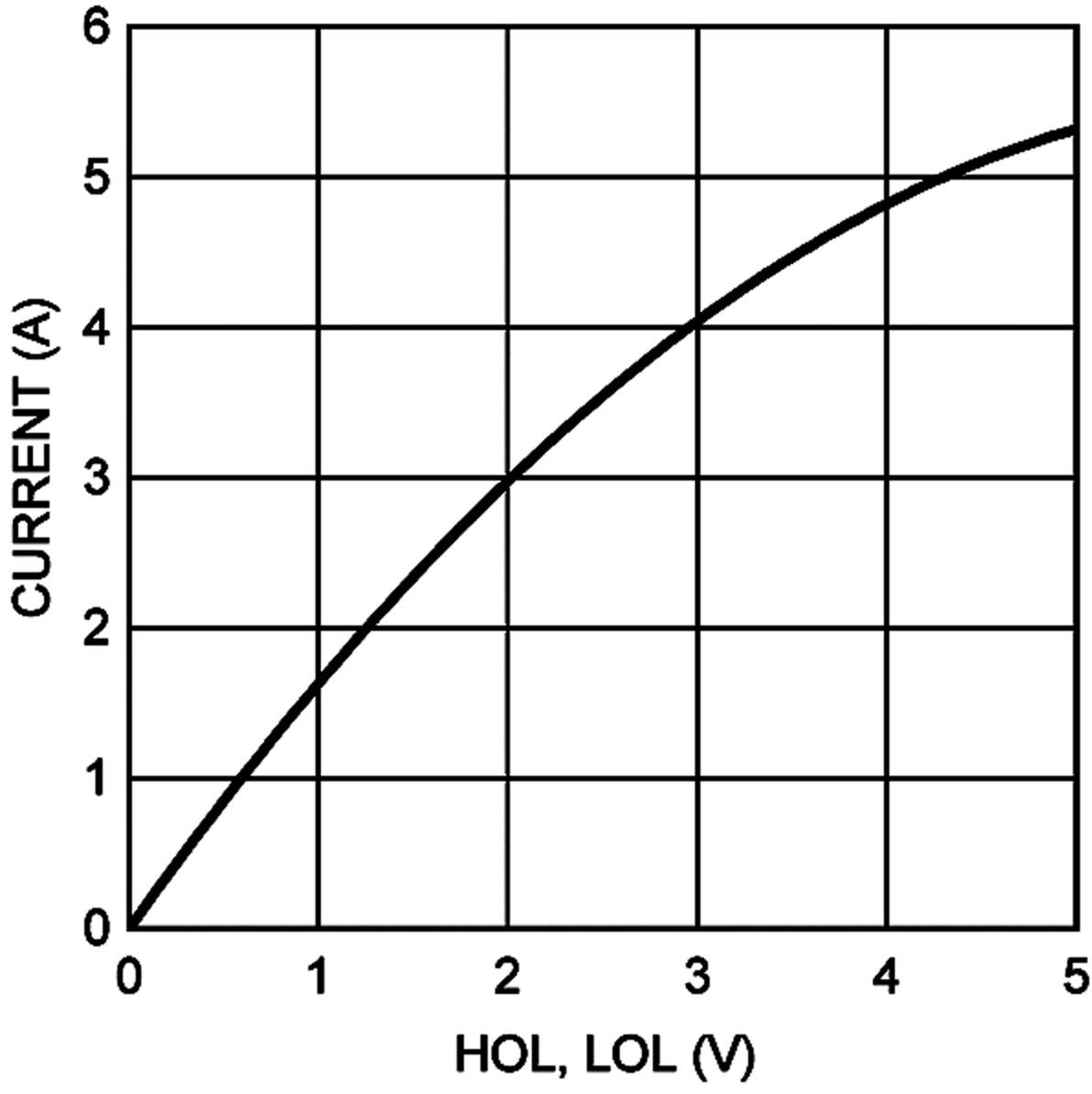 Figure 3. Peak Sink Current vs Output Voltage
  Figure 5. IHBO vs Frequency
 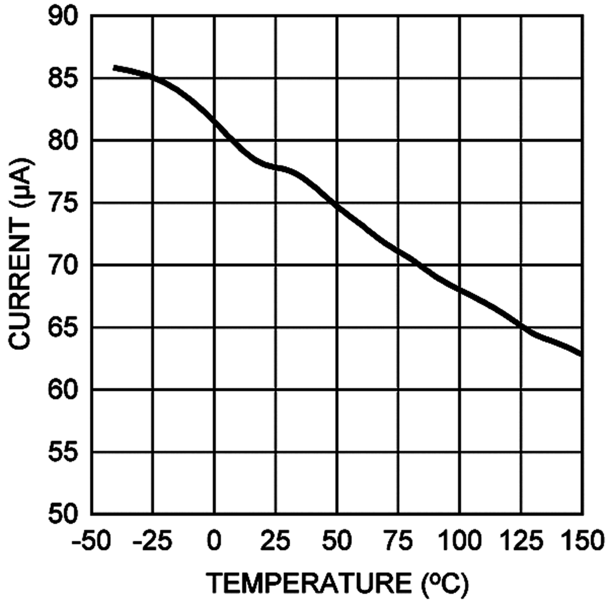 Figure 7. IHB vs Temperature
 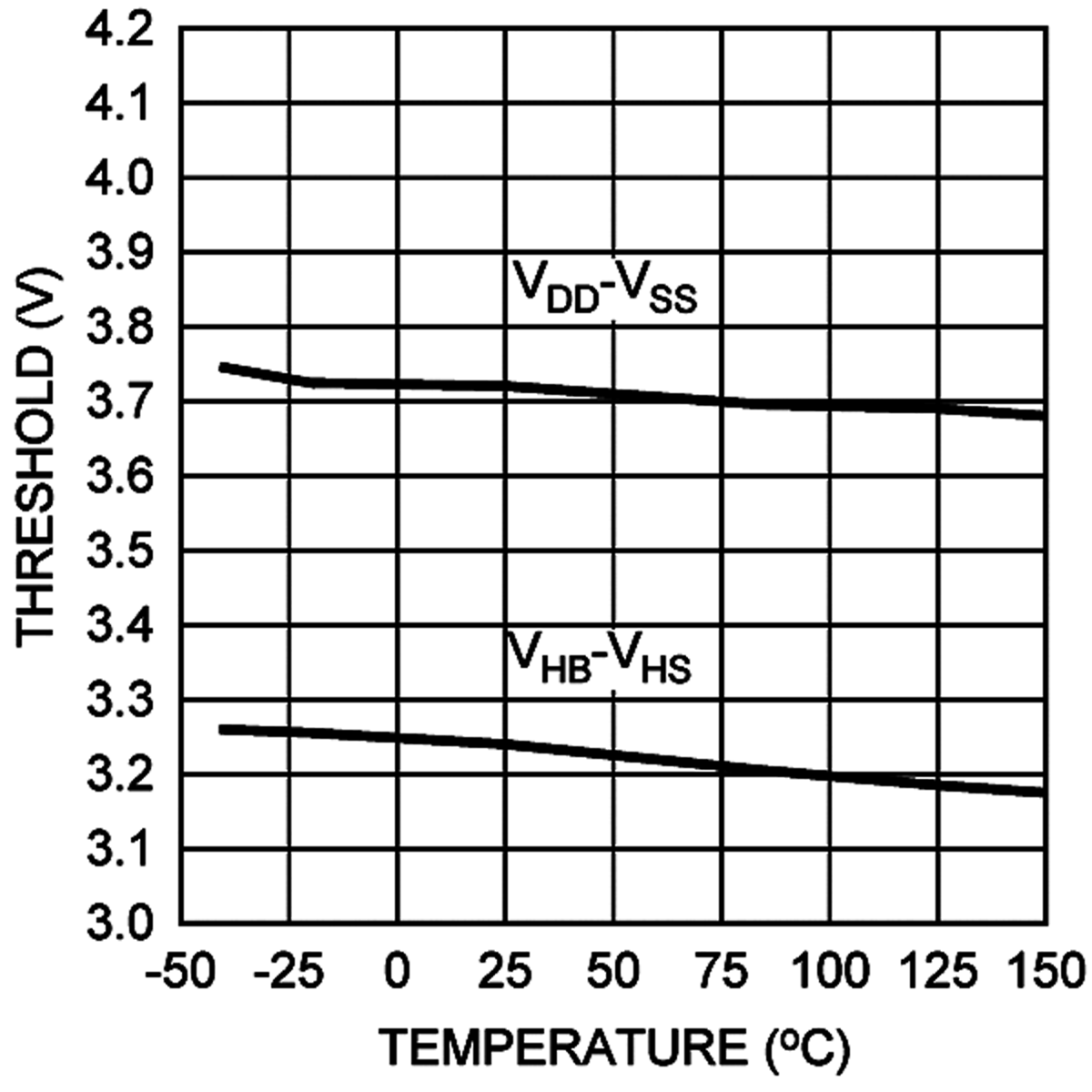 Figure 9. UVLO Falling Thresholds vs Temperature
 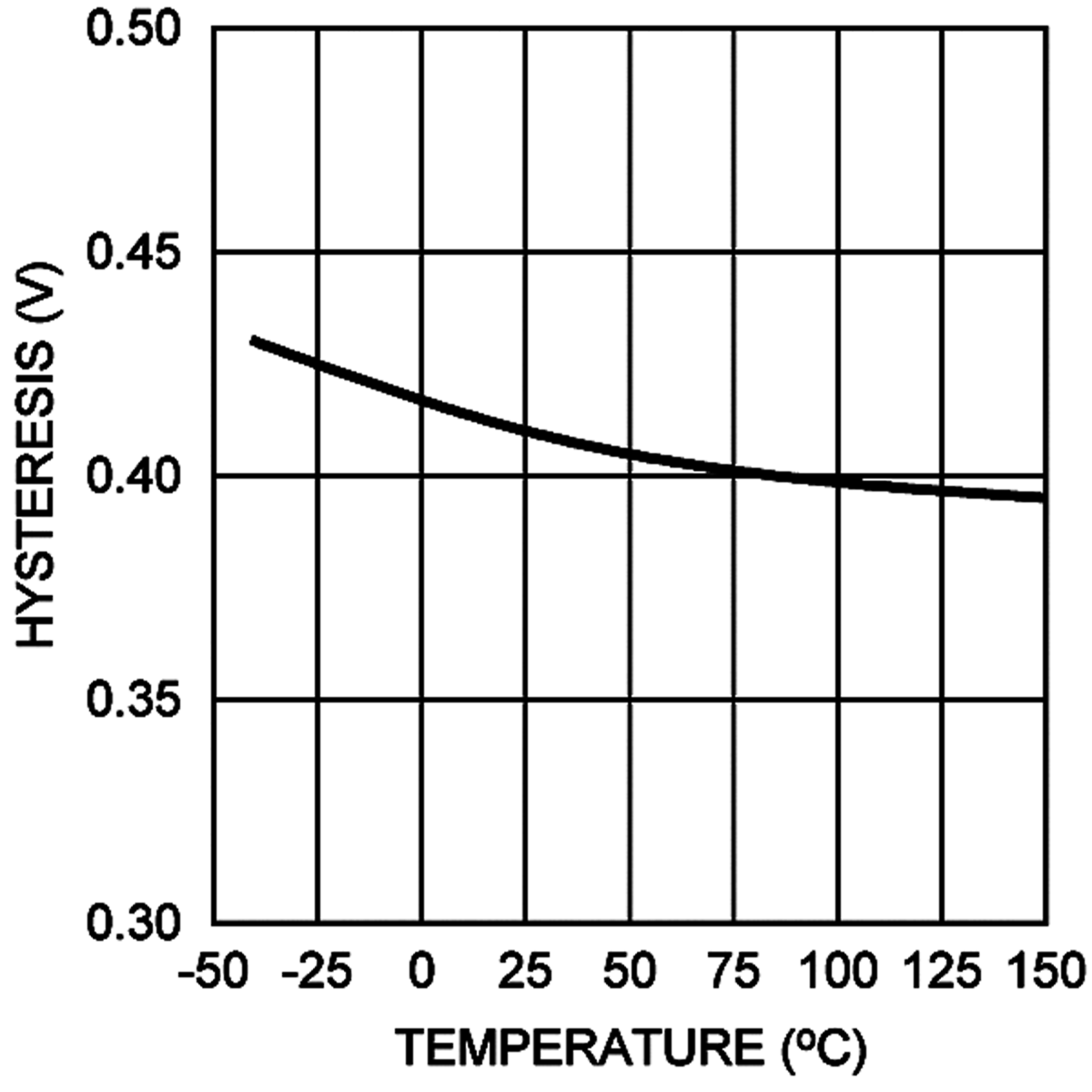 Figure 11. Input Threshold Hysteresis vs Temperature
 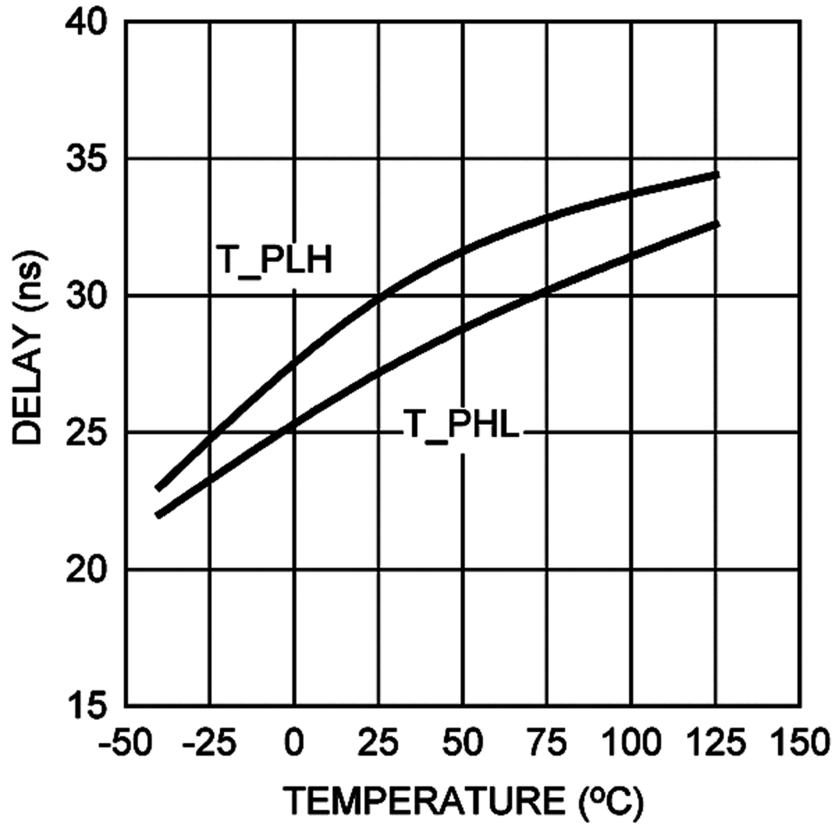 Figure 13. Propagation Delay vs Temperature
| Note: Unless otherwise specified, | ||
| VDD = VHB = 5 V, VSS = VHS = 0 V. | ||