ZHCSPC5 October 2022 LM51231-Q1
PRODUCTION DATA
- 1 特性
- 2 应用
- 3 说明
- 4 Revision History
- 5 Pin Configuration and Functions
- 6 Specifications
-
7 Detailed Description
- 7.1 Overview
- 7.2 Functional Block Diagram
- 7.3
Feature Description
- 7.3.1 Device Enable/Disable (EN, VH Pin)
- 7.3.2 High Voltage VCC Regulator (BIAS, VCC Pin)
- 7.3.3 Light Load Switching Mode Selection (MODE Pin)
- 7.3.4 VOUT Range Selection (RANGE Pin)
- 7.3.5 Line Undervoltage Lockout (UVLO Pin)
- 7.3.6 Fast Restart using VCC HOLD (VH Pin)
- 7.3.7 Adjustable Output Regulation Target (VOUT, TRK, VREF Pin)
- 7.3.8 Overvoltage Protection (VOUT Pin)
- 7.3.9 Power Good Indicator (PGOOD Pin)
- 7.3.10 Dynamically Programmable Switching Frequency (RT)
- 7.3.11 External Clock Synchronization (SYNC Pin)
- 7.3.12 Programmable Spread Spectrum (DITHER Pin)
- 7.3.13 Programmable Soft-start (SS Pin)
- 7.3.14 Wide Bandwidth Transconductance Error Amplifier and PWM (TRK, COMP Pin)
- 7.3.15 Current Sensing and Slope Compensation (CSP, CSN Pin)
- 7.3.16 Constant Peak Current Limit (CSP, CSN Pin)
- 7.3.17 Maximum Duty Cycle and Minimum Controllable On-time Limits
- 7.3.18 MOSFET Drivers, Integrated Boot Diode, and Hiccup Mode Fault Protection (LO, HO, HB Pin)
- 7.3.19 Thermal Shutdown Protection
- 7.4 Device Functional Modes
- 8 Application and Implementation
- 9 Device and Documentation Support
- 10Mechanical, Packaging, and Orderable Information
7.3.18 MOSFET Drivers, Integrated Boot Diode, and Hiccup Mode Fault Protection (LO, HO, HB Pin)
The device provides N-channel logic MOSFET drivers, which can source a peak current of 2.2 A and sink a peak current of 3.3 A. The LO driver is powered by VCC, and is enabled when EN is greater than VEN and VCC is greater than VVCC-UVLO. The HO driver is powered by HB, and is enabled when EN is greater than VEN and HB-SW voltage is greater than HB UVLO threshold (VHB-UVLO).
When the SW pin voltage is approximately 0 V by turning on the low-side MOSFET, the CHB is charged from VCC through the internal boot diode. The recommended value of the CHB is 0.1 μF.
The LO and HO outputs are controlled with an adaptive dead-time methodology which ensures that both outputs are not turned on at the same time. When the device commands LO to be turned on, the adaptive dead-time logic first turns off HO and waits for HO-SW voltage to drop. LO is then turned on after a small delay (tDHL). Similarly, the HO driver turn-on is delayed until the LO-PGND voltage has discharged. HO is then turned on after a small delay (tDLH).
If the BIAS pin voltage is below the 5-V VCC regulation target, take extra care when selecting the MOSFETs. The gate plateau voltage of the MOSFET switch must be less than the BIAS pin voltage to completely enhance the MOSFET, especially during start-up at low BIAS pin voltage. If the driver output voltage is lower than the MOSFET gate plateau voltage during start-up, the converter may not start up properly and it can stick at the maximum duty cycle in a high-power dissipation state. This condition can be avoided by selecting a lower threshold MOSFET or by turning on the device when the BIAS pin voltage is sufficient. Care should be taken when the converter operates in bypass at any conditions. During the bypass operation, the minimum HO-SW voltage is 3.75 V.
The hiccup mode fault protection is triggered by the HB UVLO. If the HB-SW voltage is less than the HB UVLO threshold (VHB-UVLO), the LO turns on by force for 75 ns to replenish the boost capacitor. The device allows up to four consecutive replenish switching. After the maximum four consecutive boot replenish switching, the device skips switching for 12 cycles. If the device fails to replenish the boost capacitor after the four sets of the four consecutive replenish switching, the device stops switching and enters 512 cycles of hiccup mode off-time. During the hiccup mode off-time, PGOOD and SS are grounded.
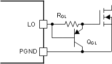
If required, the slew rate of the switching node voltage can be adjusted by adding a gate resistor in parallel with pulldown PNP transistor. Extra care should be taken when adding the gate resistor since it can decrease the effective dead-time.
 Figure 7-19 Slew Rate Control