ZHCSPC5 October 2022 LM51231-Q1
PRODUCTION DATA
- 1 特性
- 2 应用
- 3 说明
- 4 Revision History
- 5 Pin Configuration and Functions
- 6 Specifications
-
7 Detailed Description
- 7.1 Overview
- 7.2 Functional Block Diagram
- 7.3
Feature Description
- 7.3.1 Device Enable/Disable (EN, VH Pin)
- 7.3.2 High Voltage VCC Regulator (BIAS, VCC Pin)
- 7.3.3 Light Load Switching Mode Selection (MODE Pin)
- 7.3.4 VOUT Range Selection (RANGE Pin)
- 7.3.5 Line Undervoltage Lockout (UVLO Pin)
- 7.3.6 Fast Restart using VCC HOLD (VH Pin)
- 7.3.7 Adjustable Output Regulation Target (VOUT, TRK, VREF Pin)
- 7.3.8 Overvoltage Protection (VOUT Pin)
- 7.3.9 Power Good Indicator (PGOOD Pin)
- 7.3.10 Dynamically Programmable Switching Frequency (RT)
- 7.3.11 External Clock Synchronization (SYNC Pin)
- 7.3.12 Programmable Spread Spectrum (DITHER Pin)
- 7.3.13 Programmable Soft-start (SS Pin)
- 7.3.14 Wide Bandwidth Transconductance Error Amplifier and PWM (TRK, COMP Pin)
- 7.3.15 Current Sensing and Slope Compensation (CSP, CSN Pin)
- 7.3.16 Constant Peak Current Limit (CSP, CSN Pin)
- 7.3.17 Maximum Duty Cycle and Minimum Controllable On-time Limits
- 7.3.18 MOSFET Drivers, Integrated Boot Diode, and Hiccup Mode Fault Protection (LO, HO, HB Pin)
- 7.3.19 Thermal Shutdown Protection
- 7.4 Device Functional Modes
- 8 Application and Implementation
- 9 Device and Documentation Support
- 10Mechanical, Packaging, and Orderable Information
7.3.7 Adjustable Output Regulation Target (VOUT, TRK, VREF Pin)
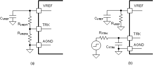
The VOUT regulation target (VOUT-REG) is adjustable by programming the TRK pin voltage which is the reference of the internal error amplifier. The accuracy of VOUT-REG is ensured when the TRK voltage is between 0.25 V and 1.0 V. If the VOUT regulation set point is set outside of the VOUT range selection, VOUT is still regulated. The high impedance TRK pin allows users to program the pin voltage directly by a D/A converter or by connecting to a resistor voltage divider (RVREFT, RVREFB) between VREF and AGND. See Figure 7-6.
The device provides a 1-V voltage reference (VREF) which can be used to program the TRK pin voltage through a resistor voltage divider. It is not recommended to use VREF as a reference voltage of an external circuit. For stability reasons the VREF capacitor (CVREF) should be between 330 pF and 1 nF, 470 pF are recommended.
When RVREFT and RVREFB are used to program the TRK pin voltage, VOUT-REG can be calculated as follows.
Lower VOUT RangeThe TRK pin voltage can be dynamically programmed in active mode, which makes an envelope tracking power supply design easy. When designing a tracking power supply, it is required to adjust the TRK pin voltage slow enough so that the VOUT pin voltage can track the command and the internal overvoltage or undervoltage comparator is not triggered during the transient operation. It is recommended to use an RC filter at the TRK pin to slow down the slew rate of the command signal at the TRK pin, especially when a step input is applied. When a trapezoidal or sinusoidal input is applied, it is recommended to limit the slew rate or the frequency of the command signal. Bypass mode, OVP and PGOOD functions are based on the TRK pin voltage, see Section 7.4.1.4, Section 7.3.8, Section 7.3.9 respectively.
 Figure 7-6 TRK Control (a) using VREF (b)
by External Step Input