ZHCSPC5 October 2022 LM51231-Q1
PRODUCTION DATA
- 1 特性
- 2 应用
- 3 说明
- 4 Revision History
- 5 Pin Configuration and Functions
- 6 Specifications
-
7 Detailed Description
- 7.1 Overview
- 7.2 Functional Block Diagram
- 7.3
Feature Description
- 7.3.1 Device Enable/Disable (EN, VH Pin)
- 7.3.2 High Voltage VCC Regulator (BIAS, VCC Pin)
- 7.3.3 Light Load Switching Mode Selection (MODE Pin)
- 7.3.4 VOUT Range Selection (RANGE Pin)
- 7.3.5 Line Undervoltage Lockout (UVLO Pin)
- 7.3.6 Fast Restart using VCC HOLD (VH Pin)
- 7.3.7 Adjustable Output Regulation Target (VOUT, TRK, VREF Pin)
- 7.3.8 Overvoltage Protection (VOUT Pin)
- 7.3.9 Power Good Indicator (PGOOD Pin)
- 7.3.10 Dynamically Programmable Switching Frequency (RT)
- 7.3.11 External Clock Synchronization (SYNC Pin)
- 7.3.12 Programmable Spread Spectrum (DITHER Pin)
- 7.3.13 Programmable Soft-start (SS Pin)
- 7.3.14 Wide Bandwidth Transconductance Error Amplifier and PWM (TRK, COMP Pin)
- 7.3.15 Current Sensing and Slope Compensation (CSP, CSN Pin)
- 7.3.16 Constant Peak Current Limit (CSP, CSN Pin)
- 7.3.17 Maximum Duty Cycle and Minimum Controllable On-time Limits
- 7.3.18 MOSFET Drivers, Integrated Boot Diode, and Hiccup Mode Fault Protection (LO, HO, HB Pin)
- 7.3.19 Thermal Shutdown Protection
- 7.4 Device Functional Modes
- 8 Application and Implementation
- 9 Device and Documentation Support
- 10Mechanical, Packaging, and Orderable Information
7.3.11 External Clock Synchronization (SYNC Pin)
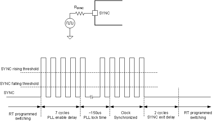
The switching frequency of the device can be synchronized to an external clock by directly applying an external pulse signal to the SYNC pin. The internal clock is synchronized at the rising edge of the external synchronization pulse using an internal PLL. Connect the SYNC pin to ground if not used.
The external synchronization pulse must be greater than VSYNC in the high logic state and must be less than VSYNC in the low logic state. The duty cycle of the external synchronization pulse is not limited, but the minimum on-pulse and the minimum off-pulse widths must be greater than 100 ns. The frequency of the external synchronization pulse must satisfy the following two inequalities.

For example, an RT resistor is required for typical 350-kHz switching to cover from 263-kHz to 525-kHz clock synchronization without changing the RT resistor.
 Figure 7-9 External Clock Synchronization
Drive the SYNC pin through a minimum 1-kΩ resistor if the BIAS pin voltage is less than the SYNC pin voltage in any conditions.