ZHCSEX5 April 2016 LM5175-Q1
PRODUCTION DATA.
- 1 特性
- 2 应用
- 3 说明
- 4 简化电路原理图
- 5 修订历史记录
- 6 Pin Configuration and Functions
- 7 Specifications
-
8 Detailed Description
- 8.1 Overview
- 8.2 Functional Block Diagram
- 8.3
Feature Description
- 8.3.1 Fixed Frequency Valley/Peak Current Mode Control with Slope Compensation
- 8.3.2 VCC Regulator and Optional BIAS Input
- 8.3.3 Enable/UVLO
- 8.3.4 Soft-Start
- 8.3.5 Overcurrent Protection
- 8.3.6 Average Input/Output Current Limiting
- 8.3.7 CCM/DCM Operation
- 8.3.8 Frequency and Synchronization (RT/SYNC)
- 8.3.9 Frequency Dithering
- 8.3.10 Output Overvoltage Protection (OVP)
- 8.3.11 Power Good (PGOOD)
- 8.3.12 Gm Error Amplifier
- 8.3.13 Integrated Gate Drivers
- 8.3.14 Thermal Shutdown
- 8.4 Device Functional Modes
-
9 Application and Implementation
- 9.1 Application Information
- 9.2
Typical Application
- 9.2.1 Design Requirements
- 9.2.2
Detailed Design Procedure
- 9.2.2.1 Frequency
- 9.2.2.2 VOUT
- 9.2.2.3 Inductor Selection
- 9.2.2.4 Output Capacitor
- 9.2.2.5 Input Capacitor
- 9.2.2.6 Sense Resistor (RSENSE)
- 9.2.2.7 Slope Compensation
- 9.2.2.8 UVLO
- 9.2.2.9 Soft-Start Capacitor
- 9.2.2.10 Dither Capacitor
- 9.2.2.11 MOSFETs QH1 and QL1
- 9.2.2.12 MOSFETs QH2 and QL2
- 9.2.2.13 Frequency Compensation
- 9.2.3 Application Curves
- 10Power Supply Recommendations
- 11Layout
- 12器件和文档支持
- 13机械、封装和可订购信息
9 Application and Implementation
NOTE
Information in the following applications sections is not part of the TI component specification, and TI does not warrant its accuracy or completeness. TI’s customers are responsible for determining suitability of components for their purposes. Customers should validate and test their design implementation to confirm system functionality.
9.1 Application Information
The LM5175-Q1 is a four-switch buck-boost controller. A quick-start tool on the LM5175-Q1 product webpage can be used to design a buck-boost converter using the LM5175-Q1. Alternatively, Webench®software can create a complete buck-boost design using the LM5175-Q1 and generate bill of materials, estimate efficiency, solution size, and cost of the complete solution. The following sections describe a detailed step-by-step design procedure for a typical application circuit.
9.2 Typical Application
A typical application example is a buck-boost converter operating from a wide input voltage range of 6 V to 36 V and providing a stable 12 V output voltage with current capability of 6 A.
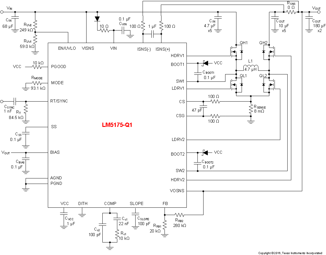 Figure 24. LM5175-Q1 Four-Switch Buck Boost Application Schematic
9.2.1 Design Requirements
For this design example, the following are used as the input parameters.
| DESIGN PARAMETER | EXAMPLE VALUE |
|---|---|
| Input Voltage Range | 6 V to 36 V |
| Output | 12 V |
| Load Current | 6 A |
| Switching Frequency | 300 kHz |
| Mode | CCM, Hiccup |
9.2.2 Detailed Design Procedure
9.2.2.1 Frequency
The switching frequency of LM5175-Q1 is set by an RT resistor connected from RT/SYNC pin to AGND. The RT resistor required to set the desired frequency is calculated using Equation 5 or Figure 3 . A 1% standard resistor of 84.5 kΩ is selected for Fsw = 300 kHz.
9.2.2.2 VOUT
The output voltage is set using a resistor divider to the FB pin. The internal reference voltage is 0.8 V. Normally the bottom resistor in the resistor divider is selected to be in the 1 kΩ to 100 kΩ range. Select

The top resistor in the feedback resistor divider is selected using Equation 12:

9.2.2.3 Inductor Selection
The inductor selection is based on consideration of both buck and boost modes of operation. For the buck mode, inductor selection is based on limiting the peak to peak current ripple ΔIL to ~40% of the maximum inductor current at the maximum input voltage. The target inductance for the buck mode is:

For the boost mode, the inductor selection is based on limiting the peak to peak current ripple ΔIL to ~40% of the maximum inductor current at the minimum input voltage. The target inductance for the boost mode is:

In this particular application, the buck inductance is larger. Choosing a larger inductance reduces the ripple current but also increases the size of the inductor. A larger inductor also reduces the achievable bandwidth of the converter by moving the right half plane zero to lower frequencies. Therefore a judicious compromise should be made based on the application requirements. For this design a 4.7-µH inductor is selected. With this inductor selection, the inductor current ripple is 5.7 A, 4.3 A, and 2.1 A, at VIN of 36 V, 24 V, and 6 V respectively.
The maximum average inductor current occurs at the minimum input voltage and maximum load current:

where a 90% efficiency is assumed. The peak inductor current occurs at minimum input voltage and is given by:

To ensure sufficient output current, the current limit threshold must be set to allow the maximum load current in boost operation. To ensure that the inductor does not saturate in current limit, the peak saturation current of the inductor should be higher than the maximum current limit. Adjusting for a ±20% current limit threshold tolerance, the peak inductor current limit is:

Therefore, the inductor saturation current should be greater than 21.6 A. If hiccup mode protection is not enabled, the RMS current rating of the inductor should be sufficient to tolerate continuous operation in cycle-by-cycle current limiting.
9.2.2.4 Output Capacitor
In the boost mode, the output capacitor conducts high ripple current. The output capacitor RMS ripple current is given by Equation 18 where the minimum VIN corresponds to the maximum capacitor current.

In this example the maximum output ripple RMS current is ICOUT(RMS) = 6 A. A 5-mΩ output capacitor ESR causes an output ripple voltage of 60 mV as given by:

A 400 µF output capacitor causes a capacitive ripple voltage of 25 mV as given by:

Typically a combination of ceramic and bulk capacitors is needed to provide low ESR and high ripple current capacity. The complete schematic in Figure 24 at the end of this section shows a good starting point for COUT for typical applications.
9.2.2.5 Input Capacitor
In the buck mode, the input capacitor supplies high ripple current. The RMS current in the input capacitor is given by:

The maximum RMS current occurs at D = 0.5, which gives ICIN(RMS) = IOUT/2 = 3 A. A combination of ceramic and bulk capacitors should be used to provide short path for high di/dt current and to reduce the output voltage ripple. The complete schematic in Figure 24 is a good starting point for CIN for typical applications.
9.2.2.6 Sense Resistor (RSENSE)
The current sense resistor between the CS and CSG pins should be selected to ensure that current limit is set high enough for both buck and boost modes of operation. For the buck operation, the current limit resistor is given by:

For the boost mode of operation, the current limit resistor is given by:

The closest standard value of RSENSE = 8 mΩ is selected based on the boost mode operation.
The maximum power dissipation in RSENSE happens at VIN(MIN):

Based on this, select the current sense resistor with power rating of 2 W or higher.
For some application circuits, it may be required to add a filter network to attenuate noise in the CS and CSG sense lines. Please see Figure 24 for typical values. The filter resistance should not exceed 100 Ω.
9.2.2.7 Slope Compensation
For stable current loop operation and to avoid sub-harmonic oscillations, the slope capacitor should be selected based on Equation 25:

This slope compensation results in “dead-beat” operation, in which the current loop disturbances die out in one switching cycle. Theoretically a current mode loop is stable with half the “dead-beat” slope (twice the calculated slope capacitor value in Equation 25). A smaller slope capacitor results in larger slope signal which is better for noise immunity in the transition region (VIN~VOUT). A larger slope signal, however, restricts the achievable input voltage range for a given output voltage, switching frequency, and inductor. For this design CSLOPE = 100 pF is selected for better transition region behavior while still providing the required VIN range. This selection of slope capacitor, inductor, switching frequency, and inductor satisfies the COMP range limitation explained in Gm Error Amplifier section.
9.2.2.8 UVLO
The UVLO resistor divider must be designed for turn-on below 6V. Selecting a RUV2 = 249 kΩ gives a UVLO hysteresis of 0.8 V. The lower UVLO resistor is the selected using Equation 26:

A standard value of 59.0 kΩ is selected for RUV1.
When programming the UVLO threshold for lower input voltage operation, it is important to choose MOSFETs with gate (Miller) plateau voltage lower than the minimum VIN.
9.2.2.9 Soft-Start Capacitor
The soft-start time is programmed using the soft-start capacitor. The relationship between CSS and the soft-start time is given by:

CSS = 0.1 µF gives a soft-start time of 16 ms.
9.2.2.10 Dither Capacitor
The dither capacitor sets the modulation frequency of the frequency dithering around the nominal switching frequency. A larger CDITH results in lower modulation frequency. For proper operation the modulation frequency (FMOD) must be much lower than the switching frequency. Use Equation 28 to select CDITH for the target modulation frequency.

For the current design dithering is not being implemented. Therefore a 0 Ω resistor from the DITH pin to AGND disables this feature.
9.2.2.11 MOSFETs QH1 and QL1
The input side MOSFETs QH1 and QL1 need to withstand the maximum input voltage of 36 V. In addition they must withstand the transient spikes at SW1 during switching. Therefore QH1 and QL1 should be rated for 60 V. The gate plateau voltages of the MOSFETs should be smaller than the minimum input voltage of the converter, otherwise the MOSFETs may not fully enhance during startup or overload conditions.
The power loss in QH1 in the boost mode of operation is approximated by:

The power loss in QH1 in the buck mode of operation consists of both conduction and switching loss components given by Equation 30 and Equation 31 respectively:


The rise (tr) and the fall (tf) times are based on the MOSFET datasheet information or measured in the lab. Typically a MOSFET with smaller RDSON (smaller conduction loss) will have longer rise and fall times (larger switching loss).
The power loss in QL1 in the buck mode of operation is given by the following equation:

9.2.2.12 MOSFETs QH2 and QL2
The output side MOSFETs QH2 and QL2 see the output voltage of 12 V and additional transient spikes at SW2 during switching. Therefore QH2 and QL2 should be rated for 20 V or more. The gate plateau voltages of the MOSFETs should be smaller than the minimum input voltage of the converter, otherwise the MOSFETs may not fully enhance during startup or overload conditions.
The power loss in QH2 in the buck mode of operation is approximated by:

The power loss in QL2 in the boost mode of operation consists of both conduction and switching loss components given by Equation 34 and Equation 35 respectively:


The rise (tr) and the fall (tf) times can be based on the MOSFET datasheet information or measured in the lab. Typically a MOSFET with smaller RDSON (lower conduction loss) has longer rise and fall times (larger switching loss).
The power loss in QH2 in the boost mode of operation is given by the following equation:

9.2.2.13 Frequency Compensation
This section presents the control loop compensation design procedure for the LM5175-Q1 buck-boost controller. The LM5175-Q1 operates mainly in buck or boost modes, separated by a transition region, and therefore the control loop design is done for both buck and boost operating modes. Then a final selection of compensation is made based on the mode that is more restrictive from a loop stability point of view. Typically for a converter designed to go deep into both buck and boost operating regions, the boost compensation design is more restrictive due to the presence of a right half plane zero (RHPZ) in the boost mode.
The boost power stage output pole location is given by:

where ROUT = 2 Ω corresponds to the maximum load of 6 A.
The boost power stage ESR zero location is given by:

The boost power stage RHP zero location is given by:

where DMAX is the maximum duty cycle at the minimum VIN.
The buck power stage output pole location is given by:

The buck power stage ESR zero location is the same as the boost power stage ESR zero.
It is clear from Equation 39 that RHP zero is the main factor limiting the achievable bandwidth. For a robust design the crossover frequency should be less than 1/3 of the RHP zero frequency. Given the position of the RHP zero, a reasonable target bandwidth in boost operation is around 4 kHz:

For some power stages, the boost RHP zero might not be as restrictive. This happens when the boost maximum duty cycle (DMAX) is small, or when a really small inductor is used. In those cases, compare the limits posed by the RHP zero (fRHP/3) with 1/20 of the switching frequency and use the smaller of the two values as the achievable bandwidth.
The compensation zero can be placed at 1.5 times the boost output pole frequency. Keep in mind that this locates the zero at 3 times the buck output pole frequency which results in approximately 30 degrees of phase loss before crossover of the buck loop and 15 degrees of phase loss at intermediate frequencies for the boost loop:

If the crossover frequency is well below the RHP zero and the compensation zero is placed well below the crossover, the compensation gain resistor Rc1 is calculated using the approximation:

where DMAX is the maximum duty cycle at the minimum VIN in boost mode and ACS is the current sense amplifier gain. The compensation capacitor Cc1 is then calculated from:

The standard values of compensation components are selected to be Rc1 = 10 kΩ and Cc1 = 22 nF.
A high frequency pole is added to suppress switching noise using a 100 pF capacitor (Cc2) in parallel with Rc1 and Cc1. These values provide a good starting point for the compensation design. Each design should be tuned in the lab to achieve the desired balance between stability margin across the operating range and transient response time.
9.2.3 Application Curves
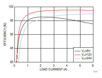 Figure 25. Efficiency vs Load
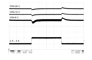 Figure 27. Load Transient Response
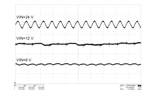 Figure 26. Output Voltage Ripple
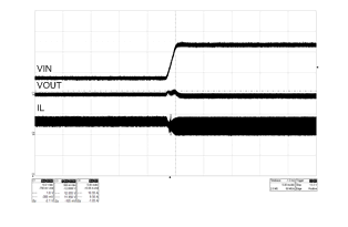 Figure 28. Line Transient Response (8 V – 24 V, IOUT = 2 A)