ZHCSEK7D June 2015 – May 2021 LM53600-Q1 , LM53601-Q1
PRODUCTION DATA
- 1 特性
- 2 应用
- 3 说明
- 4 Revision History
- 5 Device Comparison
- 6 Pin Configuration and Functions
- 7 Specifications
- 8 Detailed Description
- 9 Applications and Implementation
- 10Power Supply Recommendations
- 11Layout
- 12Device and Documentation Support
- 13Mechanical, Packaging, and Orderable Information
11.1 Layout Guidelines
The following list is in order of importance starting with the most important item:-
- Place high frequency input bypass capacitor, Cinhf, as close to the LM53600-Q1 and LM53601-Q1 devices as possible.
- Connect AGND and GND to the DAP immediately adjacent to the LM53600-Q1 and LM53601-Q1 devices.
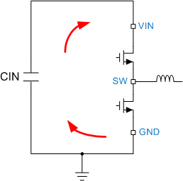
- Do not interrupt the ground plain under the loop containing the VIN and GND pins and Cinhf of the LM53600-Q1 and LM53601-Q1 devices.
- The boot capacitor, CBOOT, should be close to the LM53601-Q1 and the loop from the SW pin, through the boot capacitor and into the BOOT pin should be kept as small as possible.
- Keep the SW node as small as possible. It should be wide enough to carry the converter’s full current without significant drop.
- 4.7 µF of bypassing should be close to the input of the LM53600-Q1 and LM53601-Q1 devices.
- Place CVCC, the VCC pin’s bypass, and CBIAS, the bypass for FB for fixed voltage devices and BIAS for adjustable devices as close to the LM53600-Q1 and LM53601-Q1 devices as possible.
- The first output the trace from the output inductor to the output node should run by an output capacitor before joining the rest of the output node.
- Keep 10 µF close to the output (output inductor and GND) of the LM53600-Q1 and LM53601-Q1 devices.
- Clear the layer beneath the SW node.
Table 11-1 PCB Layout Resources
| TITLE | LINK |
|---|---|
| AN-1149 Layout Guidelines for Switching Power Supplies | SNVA021 |
| AN-1229 Simple Switcher PCB Layout Guidelines | SNVA054 |
| Constructing Your Power Supply- Layout Considerations | SLUP230 |
| SNVA721 Low Radiated EMI Layout Made SIMPLE with LM4360x and LM4600x | SNVA721 |
 Figure 11-1 Current Loops with Fast Transients