ZHCSOW5B September   2021  – July 2022 LM74721-Q1

PRODUCTION DATA  

  1. 特性
  2. 应用
  3. 说明
  4. Revision History
  5. Pin Configuration and Functions
  6. Specifications
    1. 6.1 Absolute Maximum Ratings
    2. 6.2 ESD Ratings
    3. 6.3 Recommended Operating Conditions
    4. 6.4 Thermal Information
    5. 6.5 Electrical Characteristics
    6. 6.6 Switching Characteristics
    7. 6.7 Typical Characteristics
  7. Parameter Measurement Information
  8. Detailed Description
    1. 8.1 Overview
    2. 8.2 Functional Block Diagram
    3. 8.3 Feature Description
      1. 8.3.1 Reverse Battery Protection (A, C, GATE)
        1. 8.3.1.1 Input TVS Less Operation: VDS Clamp
      2. 8.3.2 Load Disconnect Switch Control (PD)
      3. 8.3.3 Overvoltage Protection and Battery Voltage Sensing (VSNS, SW, OV)
      4. 8.3.4 Boost Regulator
    4. 8.4 Shutdown Mode
  9. Application and Implementation
    1. 9.1 Application Information
    2. 9.2 Typical 12-V Reverse Battery Protection Application
      1. 9.2.1 Design Requirements for 12-V Battery Protection
      2. 9.2.2 Detailed Design Procedure
        1. 9.2.2.1 Boost Converter Components (C2, C3, L1)
        2. 9.2.2.2 Input and Output Capacitance
        3. 9.2.2.3 Hold-Up Capacitance
        4. 9.2.2.4 MOSFET Selection: Q1
      3. 9.2.3 Application Curves
    3. 9.3 What to Do and What Not to Do
  10. 10Power Supply Recommendations
    1. 10.1 Transient Protection
  11. 11Layout
    1. 11.1 Layout Guidelines
    2. 11.2 Layout Example
  12. 12Device and Documentation Support
    1. 12.1 接收文档更新通知
    2. 12.2 支持资源
    3. 12.3 Trademarks
    4. 12.4 Electrostatic Discharge Caution
    5. 12.5 术语表
  13. 13Mechanical, Packaging, and Orderable Information

封装选项

请参考 PDF 数据表获取器件具体的封装图。

机械数据 (封装 | 引脚)
  • DRR|12
散热焊盘机械数据 (封装 | 引脚)
订购信息

Transient Protection

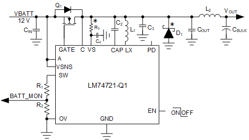
When the MOSFET is turned OFF during conditions such as reverse current blocking in the system designs where there is an output C-L-C filter (for EMI filtering) as shown in Figure 10-1, the voltage across COUT can swing negative based on the values of L2 ,COUT and the initial reverse current in L2 before the MOSFET turns OFF. Use a low VF Schottky diode D1 across COUT to GND and place a R-C filter with 100 Ω and 0.1 µF at Vs pin, ensuring the device pins does not exceed the Absolute Maximum Ratings.
GUID-20210429-CA0I-VX3X-KGFX-ZK7PFPC406NS-low.gif
* Optional components needed for suppression of transients
Figure 10-1 Circuit Implementation with Optional Protection Components for LM74721-Q1