SNOS738I April   1995  – January 2017 LM9061 , LM9061-Q1

PRODUCTION DATA.  

  1. Features
  2. Applications
  3. Description
  4. Revision History
  5. Pin Configuration and Functions
  6. Specifications
    1. 6.1 Absolute Maximum Ratings
    2. 6.2 ESD Ratings: LM9061
    3. 6.3 ESD Ratings: LM9061-Q1
    4. 6.4 Recommended Operating Conditions
    5. 6.5 Thermal Information
    6. 6.6 Electrical Characteristics
    7. 6.7 Switching Characteristics
    8. 6.8 Typical Characteristics
  7. Detailed Description
    1. 7.1 Overview
    2. 7.2 Functional Block Diagram
    3. 7.3 Feature Description
      1. 7.3.1 MOSFET Gate Drive
      2. 7.3.2 Basic Operation
      3. 7.3.3 Turn On and Turn Off Characteristics
      4. 7.3.4 Lossless Overcurrent Protection
      5. 7.3.5 Delay Timer
        1. 7.3.5.1 Minimum Delay Time
      6. 7.3.6 Overvoltage Protection
      7. 7.3.7 Reverse Battery
      8. 7.3.8 Low Battery
      9. 7.3.9 Increasing MOSFET Turnon Time
    4. 7.4 Device Functional Modes
      1. 7.4.1 Operation With VCC > 30 V
      2. 7.4.2 Operation With VCC < 6.2 V
      3. 7.4.3 Operation With ON/OFF Control
      4. 7.4.4 MOSFET Latch-OFF
  8. Application and Implementation
    1. 8.1 Application Information
    2. 8.2 Typical Applications
      1. 8.2.1 TITLE NEEDED
        1. 8.2.1.1 Design Requirements
        2. 8.2.1.2 Detailed Design Procedure
        3. 8.2.1.3 Application Curves
      2. 8.2.2 Bidirectional Applications
        1. 8.2.2.1 Back-to-Back MOSFET Configuration
          1. 8.2.2.1.1 Application Curve
        2. 8.2.2.2 Bidirectional Switch With Reverse Overcurrent Protection
          1. 8.2.2.2.1 Application Curve
  9. Power Supply Recommendations
  10. 10Layout
    1. 10.1 Layout Guidelines
    2. 10.2 Layout Examples
  11. 11Device and Documentation Support
    1. 11.1 Documentation Support
      1. 11.1.1 Related Documentation
    2. 11.2 Related Links
    3. 11.3 Receiving Notification of Documentation Updates
    4. 11.4 Community Resources
    5. 11.5 Trademarks
    6. 11.6 Electrostatic Discharge Caution
    7. 11.7 Glossary
  12. 12Mechanical, Packaging, and Orderable Information

封装选项

机械数据 (封装 | 引脚)
散热焊盘机械数据 (封装 | 引脚)
订购信息

Layout

Layout Guidelines

  1. The bypass capacitor for VCC must be placed as close as possible to the VCC pin.
  2. The resistor RREF must be placed as close as possible to the IREF and Ground pins with minimal trace length to keep the IREF current as accurate as possible. The LM9061 is optimized for use with a 15.4 kΩ ±1% resistor for RREF.
  3. In applications where the VCC supply is subject to high levels of transient noise, a bypass capacitor across RREF is recommended. This bypass capacitor must be no larger than 0.1 μF and must be placed as close as possible to the IREF pin.
  4. The RTHRESHOLD and RSENSE resistors must be placed as close as possible to the MOSFET drain and source pins respectively. This allows accurate monitoring of the VDS voltage across the MOSFET.
  5. An array of vias can be placed along the high current path to the output load. These vias can help conduct heat to any inner plane areas or to a bottom-side copper plane.

Layout Examples

Figure 26 and Figure 27 are layout examples for the LM9061 and LM9061-Q1. These examples are taken from the LM9061EVM. For information on the operation and schematic of the EVM, see LM9061 High-Side Protection Controller EVM (SNOU132).
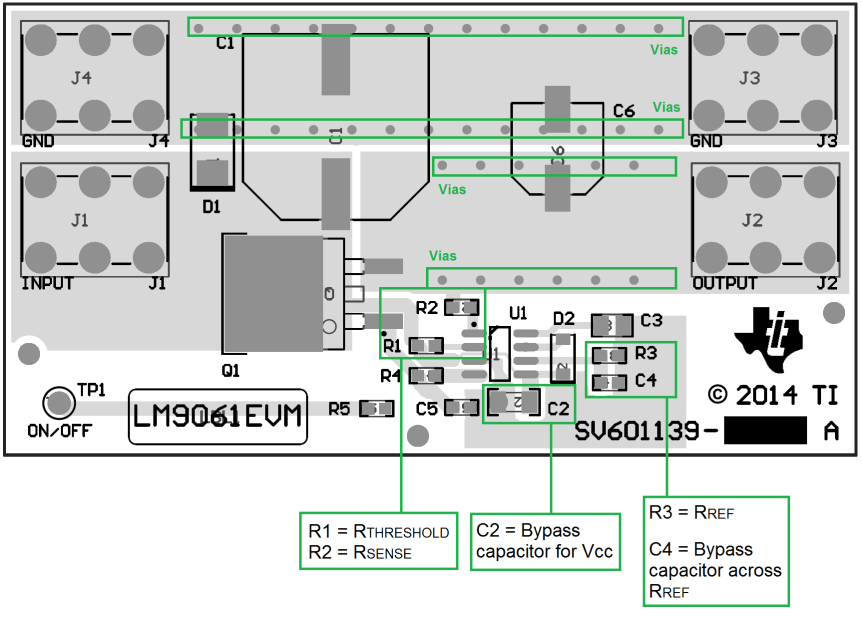
LM9061 LM9061-Q1 LM9061EVMLayoutExampleTop.gif Figure 26. LM9061EVM Layout Example (Top)
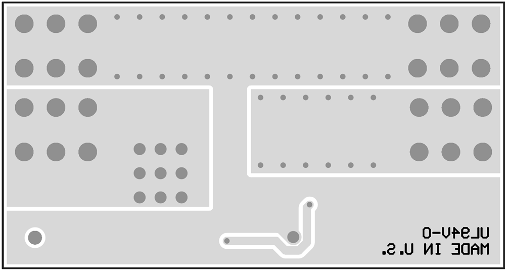
LM9061 LM9061-Q1 bottom-better.png Figure 27. LM9061EVM Layout Example (Bottom)