ZHCSJO3B May 2019 – November 2020 LMR34215-Q1
PRODUCTION DATA
- 1 特性
- 2 应用
- 3 说明
- 4 Revision History
- 5 Device Comparison Table
- 6 Pin Configuration and Functions
- 7 Specifications
- 8 Detailed Description
- 9 Power Supply Recommendations
- 10Layout
- 11Device and Documentation Support
- 12Mechanical, Packaging, and Orderable Information
9.2 Typical Application
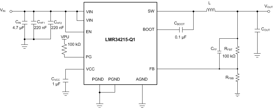
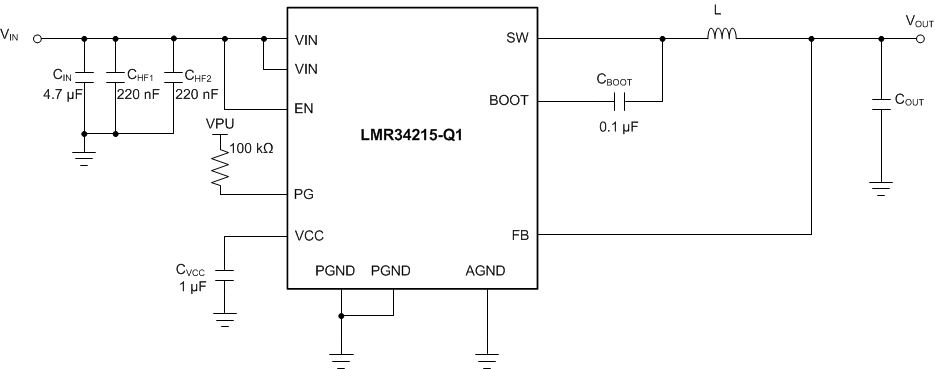
Figure 9-1 and Figure 9-2 show for the LMR34215-Q1. This device is designed to function over a wide range of external components and system parameters. However, the internal compensation is optimized for a certain range of external inductance and output capacitance. As a quick start guide, Table 9-1 provides typical component values for a range of the most common output voltages.
 Figure 9-1 Example Applications Circuit (Adjustable Output)
 Figure 9-2 Example Applications Circuit (Fixed 5-V Output)
Table 9-1 Typical External Component Values
| ƒSW (kHz) | VOUT (V) | L (µH) | NOMINAL COUT (RATED CAPACITANCE) (1) | MINIMUM COUT (RATED CAPACITANCE) (2) | RFBT (Ω) | RFBB (Ω) | CIN | CFF |
|---|---|---|---|---|---|---|---|---|
| 400 | 3.3 | 10 | 2 × 47 µF | 2 × 22 µF | 100 k | 43.2 k | 4.7 µF + 2 × 220 nF | 20 pF |
| 400 | 5 | 15 | 3 × 22 µF | 2 × 22 µF | 100 k | 24.9 k | 4.7 µF + 2 × 220 nF | 20 pF |
| 2100 | 5 | 2.2 | 2 × 22 µF | 2 × 15 µF | DNP | DNP | 4.7 µF + 2 × 220 nF | DNP |
| 400 | 12 | 27 | 3 × 22 µF | 2 × 22 µF | 100 k | 9.09 k | 4.7 µF + 2 × 220 nF | 20 pF |
(1) Optimized for superior load
transient performance from 0 to 100% rated load.
(2) Optimized for size constrained end
applications.