ZHCSM75U August 1999 – October 2020 LMV331 , LMV339 , LMV393
PRODUCTION DATA
- 1 特性
- 2 应用
- 3 说明
- 4 Revision History
- 5 Pin Configuration and Functions
-
6 Specifications
- 6.1 Absolute Maximum Ratings
- 6.2 ESD Ratings
- 6.3 Recommended Operating Conditions
- 6.4 Thermal Information
- 6.5 Electrical Characteristics, VCC+ = 2.7 V
- 6.6 Electrical Characteristics, VCC+ = 5 V
- 6.7 Switching Characteristics, VCC+ = 2.7 V
- 6.8 Switching Characteristics, VCC+ = 5 V
- 6.9 Typical Characteristics
- 7 Detailed Description
- 8 Application and Implementation
- 9 Power Supply Recommendations
- 10Layout
- 11Device and Documentation Support
- 12Mechanical, Packaging, and Orderable Information
封装选项
请参考 PDF 数据表获取器件具体的封装图。
机械数据 (封装 | 引脚)
- RUC|14
- D|14
- PW|14
散热焊盘机械数据 (封装 | 引脚)
- RUC|14
订购信息
8.2.3 Application Curves
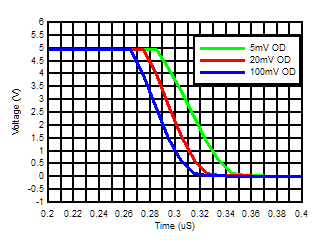
The following curves were generated with 5 V on VCC and VLogic, RPULLUP = 5.1 kΩ, and 50 pF scope probe.
 Figure 8-2 Response Time for Various Overdrives (Negative Transition)