ZHCSEK3G December 2015 – August 2022 LMX2592
PRODUCTION DATA
- 1 特性
- 2 应用
- 3 说明
- 4 Revision History
- 5 Pin Configuration and Functions
- 6 Specifications
- 7 Detailed Description
-
8 Application and Implementation
- 8.1
Application Information
- 8.1.1 Optimization of Spurs
- 8.1.2 Configuring the Input Signal Path
- 8.1.3 Input Pin Configuration
- 8.1.4 Using the OSCin Doubler
- 8.1.5 Using the Input Signal Path Components
- 8.1.6 Designing for Output Power
- 8.1.7 Current Consumption Management
- 8.1.8 Decreasing Lock Time
- 8.1.9 Modeling and Understanding PLL FOM and Flicker Noise
- 8.1.10 External Loop Filter
- 8.2 Typical Application
- 8.3 Power Supply Recommendations
- 8.4 Layout
- 8.1
Application Information
- 9 Device and Documentation Support
- 10Mechanical, Packaging, and Orderable Information
封装选项
请参考 PDF 数据表获取器件具体的封装图。
机械数据 (封装 | 引脚)
- RHA|40
散热焊盘机械数据 (封装 | 引脚)
- RHA|40
订购信息
5 Pin Configuration and Functions
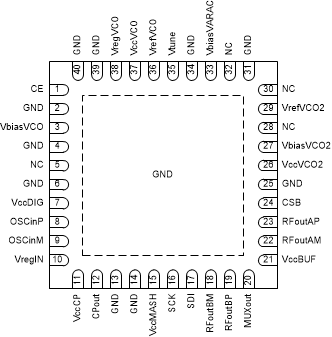
 Figure 5-1 RHA
Package40-Pin VQFNTop View
Figure 5-1 RHA
Package40-Pin VQFNTop ViewTable 5-1 Pin Functions
| PIN | TYPE | DESCRIPTION | |
|---|---|---|---|
| NAME | NO. | ||
| CE | 1 | Input | Chip Enable input. Active high powers on the device. |
| CPout | 12 | Output | Charge pump output. Recommend connecting C1 of loop filter close to pin. |
| CSB | 24 | Input | SPI chip select bar or uWire latch enable (abbreviated as LE in Figure 6-1). High impedance CMOS input. 1.8 to 3.3-V logic. |
| DAP | GND | Ground | RFout ground. |
| GND | 2, 4, 6, 13, 14, 25, 31, 34, 39, 40 | Ground | VCO ground. |
| MUXout | 20 | Output | Programmable with register MUXOUT_SEL to be readback SDO or lock detect indicator (active high). |
| NC | 5, 28, 30, 32 | — | Not connected. |
| OSCinP | 8 | Input | Differential reference input clock (+). High input impedance. Requires connecting series capacitor (0.1-µF recommended). |
| OSCinM | 9 | Input | Differential reference input clock (–). High input impedance. Requires connecting series capacitor (0.1-µF recommended). |
| RFoutAM | 22 | Output | Differential output A (–). This output requires a pullup component for proper biasing. A 50-Ω resistor or inductor may be used. Place as close to output as possible. |
| RFoutAP | 23 | Output | Differential output A (+). This output requires a pullup component for proper biasing. A 50-Ω resistor or inductor may be used. Place as close to output as possible. |
| RFoutBP | 19 | Output | Differential output B (+). This output requires a pullup component for proper biasing. A 50-Ω resistor or inductor may be used. Place as close to output as possible. |
| RFoutBM | 18 | Output | Differential output B (–). This output requires a pullup component for proper biasing. A 50-Ω resistor or inductor may be used. Place as close to output as possible. |
| SCK | 16 | Input | SPI or uWire clock (abbreviated as CLK in Figure 6-1). High impedance CMOS input. 1.8 to 3.3-V logic. |
| SDI | 17 | Input | SPI or uWire data (abbreviated as DATA in Figure 6-1). High impedance CMOS input. 1.8 to 3.3-V logic. |
| VbiasVARAC | 33 | Bypass | VCO varactor internal voltage, access for bypass. Requires connecting 10-µF capacitor to VCO ground. |
| VbiasVCO | 3 | Bypass | VCO bias internal voltage, access for bypass. Requires connecting 10-µF capacitor to VCO ground. Place close to pin. |
| VbiasVCO2 | 27 | Bypass | VCO bias internal voltage, access for bypass. Requires connecting 1-µF capacitor to VCO ground. |
| VCCBUF | 21 | Supply | Output buffer supply. Requires connecting 0.1-µF capacitor to RFout ground. |
| VCCCP | 11 | Supply | Charge pump supply. Recommend connecting 0.1-µF capacitor to charge pump ground. |
| VCCDIG | 7 | Supply | Digital supply. Recommend connecting 0.1-µF capacitor to digital ground. |
| VCCMASH | 15 | Supply | Digital supply. Recommend connecting 0.1-µF and 10-µF capacitor to digital ground. |
| VCCVCO | 37 | Supply | VCO supply. Recommend connecting 0.1-µF and 10-µF capacitor to ground. |
| VCCVCO2 | 26 | Supply | VCO supply. Recommend connecting 0.1-µF and 10-µF capacitor to VCO ground. |
| VrefVCO | 36 | Bypass | VCO supply internal voltage, access for bypass. Requires connecting 10-µF capacitor to ground. |
| VrefVCO2 | 29 | Bypass | VCO supply internal voltage, access for bypass. Requires connecting 10-µF capacitor to VCO ground. |
| VregIN | 10 | Bypass | Input reference path internal voltage, access for bypass. Requires connecting 1-µF capacitor to ground. Place close to pin. |
| VregVCO | 38 | Bypass | VCO supply internal voltage, access for bypass. Requires connecting 1-µF capacitor to ground. |
| Vtune | 35 | Input | VCO tuning voltage input. This signal should be kept away from noise sources. Connect a 3.3-nF or more capacitor to VCO ground. |