SNVS345G June   2006  – December 2014 LP5951

PRODUCTION DATA.  

  1. Features
  2. Applications
  3. Description
  4. Revision History
  5. Pin Configuration and Functions
  6. Specifications
    1. 6.1 Absolute Maximum Ratings
    2. 6.2 ESD Ratings
    3. 6.3 Recommended Operating Conditions
    4. 6.4 Thermal Information
    5. 6.5 Electrical Characteristics
    6. 6.6 Enable Control Characteristics
    7. 6.7 Transient Characteristics
    8. 6.8 Output Capacitor, Recommended Specification
    9. 6.9 Typical Characteristics
  7. Detailed Description
    1. 7.1 Overview
    2. 7.2 Functional Block Diagram
    3. 7.3 Feature Description
      1. 7.3.1 No-Load Stability
      2. 7.3.2 Enable Operation
      3. 7.3.3 Fast Turn Off And On
      4. 7.3.4 Short-Circuit Protection
      5. 7.3.5 Thermal-Overload Protection
      6. 7.3.6 Reverse Current Path
    4. 7.4 Device Functional Modes
      1. 7.4.1 Enable (EN)
      2. 7.4.2 Minimum Operating Input Voltage (VIN)
  8. Application and Implementation
    1. 8.1 Application Information
    2. 8.2 Typical Application
      1. 8.2.1 Design Requirements
      2. 8.2.2 Detailed Design Procedure
        1. 8.2.2.1 Power Dissipation And Device Operation
        2. 8.2.2.2 External Capacitors
        3. 8.2.2.3 Input Capacitor
        4. 8.2.2.4 Output Capacitor
        5. 8.2.2.5 Capacitor Characteristics
      3. 8.2.3 Application Curves
  9. Power Supply Recommendations
    1. 9.1 Output Current Derating
  10. 10Layout
    1. 10.1 Layout Guidelines
    2. 10.2 Layout Example
  11. 11Device and Documentation Support
    1. 11.1 Device Support
      1. 11.1.1 Third-Party Products Disclaimer
    2. 11.2 Documentation Support
      1. 11.2.1 Related Documentation
    3. 11.3 Trademarks
    4. 11.4 Electrostatic Discharge Caution
    5. 11.5 Glossary
  12. 12Mechanical, Packaging, and Orderable Information

封装选项

机械数据 (封装 | 引脚)
散热焊盘机械数据 (封装 | 引脚)
订购信息

5 Pin Configuration and Functions

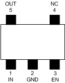
SOT-23 (DBV)
5 Pins
Top View
20136202.gif
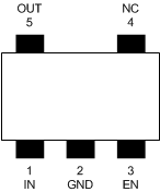
SC70 (DCK)
5 Pins
Top View
20136203.gif

Pin Functions

PIN TYPE DESCRIPTION
NUMBER NAME
1 IN I Input voltage 1.8 V to 5.5 V
2 GND Ground
3 EN I Enable pin logic input: Low = shutdown, High = normal operation. This pin should not be left floating.
4 NC No internal connection
5 OUT O Regulated output voltage