SBOS426D November 2008 – October 2016 OPA209 , OPA2209 , OPA4209
PRODUCTION DATA.
- 1 Features
- 2 Applications
- 3 Description
- 4 Revision History
- 5 Pin Configuration and Functions
- 6 Specifications
- 7 Detailed Description
- 8 Application and Implementation
- 9 Power Supply Recommendations
- 10Layout
- 11Device and Documentation Support
- 12Mechanical, Packaging, and Orderable Information
封装选项
机械数据 (封装 | 引脚)
散热焊盘机械数据 (封装 | 引脚)
订购信息
7 Detailed Description
7.1 Overview
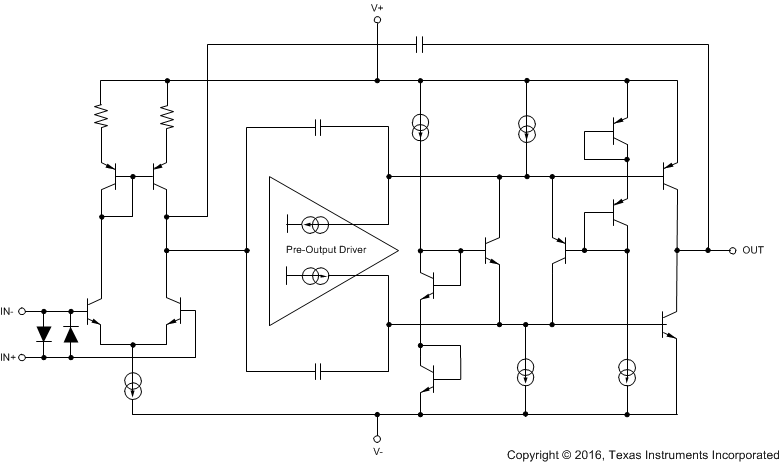
The OPA209 series of precision operational amplifiers are unity-gain stable, and free from unexpected output and phase reversal. Applications with noisy or high-impedance power supplies require decoupling capacitors placed close to the device pins. In most cases, 0.1-µF capacitors are adequate. The Functional Block Diagram shows a simplified schematic of the OPA209. This die uses a SiGe bipolar process and contains 180 transistors.
7.2 Functional Block Diagram

7.3 Feature Description
7.3.1 Operating Voltage
The OPA209 series of op amps can be used with single or dual supplies within an operating range of VS = 4.5 V (±2.25 V) up to 36 V (±18 V). Supply voltages higher than 40 V total can permanently damage the device (see Absolute Maximum Ratings).
In addition, key parameters are assured over the specified temperature range, TA = –40°C to 125°C. Parameters that vary significantly with operating voltage or temperature are shown in the Typical Characteristics.
7.3.2 Input Protection
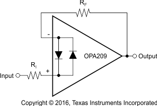
The input terminals of the OPA209 are protected from excessive differential voltage with back-to-back diodes, as shown in Figure 31. In most circuit applications, the input protection circuitry has no consequence. However, in low-gain or G = 1 circuits, fast ramping input signals can forward-bias these diodes because the output of the amplifier cannot respond rapidly enough to the input ramp. This effect is illustrated in Figure 25 and Figure 26 in Typical Characteristics. If the input signal is fast enough to create this forward-bias condition, the input signal current must be limited to 10 mA or less. If the input signal current is not inherently limited, an input series resistor can be used to limit the signal input current. This input series resistor degrades the low-noise performance of the OPA209. See Noise Performance for further information on noise performance.
Figure 31 shows an example configuration that implements a current-limiting feedback resistor.
 Figure 31. Pulsed Operation
7.3.3 Noise Performance
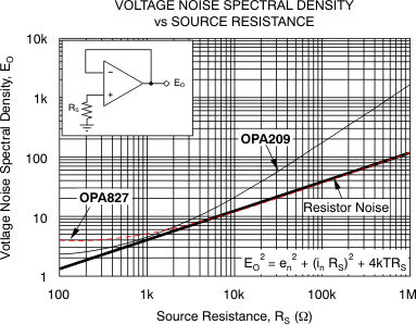
Figure 32 shows the total circuit noise for varying source impedances with the op amp in a unity-gain configuration (no feedback resistor network, and therefore no additional noise contributions). Two different op amps are shown with the total circuit noise calculated. The OPA209 has very low voltage noise, making it ideal for low source impedances (less than 2 kΩ). As a comparable precision FET-input op amp (very low current noise), the OPA827 has somewhat higher voltage noise, but lower current noise. It provides excellent noise performance at moderate to high source impedance (10 kΩ and up). For source impedance lower than 300 Ω, the OPA211 may provide lower noise.
The equation in Figure 32 shows the calculation of the total circuit noise, with these parameters:
- en = voltage noise,
- in = current noise,
- RS = source impedance,
- k = Boltzmann's constant = 1.38 × 10⁻²³ J/K, and
- T = temperature in Kelvins
For more details on calculating noise, see Basic Noise Calculations.
 Figure 32. Noise Performance of the OPA209 and OPA827 in Unity-Gain Buffer Configuration
7.3.4 Basic Noise Calculations
Low-noise circuit design requires careful analysis of all noise sources. External noise sources can dominate in many cases; consider the effect of source resistance on overall op amp noise performance. Total noise of the circuit is the root-sum-square combinations of all noise components.
The resistive portion of the source impedance produces thermal noise proportional to the square root of the resistance. This function is illustrated in Figure 32. The source impedance is usually fixed; consequently, select the appropriate op amp and the feedback resistors to minimize the respective contributions to the total noise.
Figure 33 illustrates both noninverting (Figure 33a) and inverting (Figure 33b) op amp circuit configurations with gain. In circuit configurations with gain, the feedback network resistors also contribute noise. The current noise of the op amp reacts with the feedback resistors to create additional noise components.
The feedback resistor values can generally be chosen to make these noise sources negligible. Note that low-impedance feedback resistors load the output of the amplifier. The equations for total noise are shown for both configurations.

7.3.5 Electrical Overstress
Designers often ask questions about the capability of an operational amplifier to withstand electrical overstress. These questions tend to focus on the device inputs, but may involve the supply voltage pins or even the output pin. Each of these different pin functions have electrical stress limits determined by the voltage breakdown characteristics of the particular semiconductor fabrication process and specific circuits connected to the pin. Additionally, internal electrostatic discharge (ESD) protection is built into these circuits to protect them from accidental ESD events both before and during product assembly.
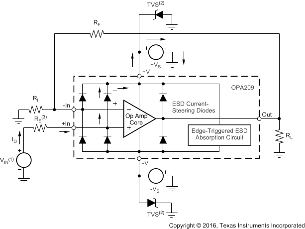
It is helpful to have a good understanding of this basic ESD circuitry and its relevance to an electrical overstress event. See Figure 34 for an illustration of the ESD circuits contained in the OPA209 series (indicated by the dashed line area). The ESD protection circuitry involves several current-steering diodes connected from the input and output pins and routed back to the internal power-supply lines, where they meet at an absorption device internal to the operational amplifier. This protection circuitry is intended to remain inactive during normal circuit operation.
An ESD event produces a short duration, high-voltage pulse that is transformed into a short duration, high-current pulse as it discharges through a semiconductor device. The ESD protection circuits are designed to provide a current path around the operational amplifier core to prevent it from being damaged. The energy absorbed by the protection circuitry is then dissipated as heat.
When an ESD voltage develops across two or more of the amplifier device pins, current flows through one or more of the steering diodes. Depending on the path that the current takes, the absorption device may activate. The absorption device has a trigger, or threshold voltage, that is above the normal operating voltage of the OPA209 but below the device breakdown voltage level. Once this threshold is exceeded, the absorption device quickly activates and clamps the voltage across the supply rails to a safe level.
When the operational amplifier connects into a circuit such as the one Figure 34 shows, the ESD protection components are intended to remain inactive and not become involved in the application circuit operation. However, circumstances may arise where an applied voltage exceeds the operating voltage range of a given pin. If this condition occur, there is a risk that some of the internal ESD protection circuits may be biased on, and conduct current. Any such current flow occurs through steering diode paths and rarely involves the absorption device.
Figure 34 depicts a specific example where the input voltage, VIN, exceeds the positive supply voltage (+VS) by 500 mV or more. Much of what happens in the circuit depends on the supply characteristics. If +VS can sink the current, one of the upper input steering diodes conducts and directs current to +VS. Excessively high current levels can flow with increasingly higher VIN. As a result, the datasheet specifications recommend that applications limit the input current to 10 mA.
If the supply is not capable of sinking the current, VIN may begin sourcing current to the operational amplifier, and then take over as the source of positive supply voltage. The danger in this case is that the voltage can rise to levels that exceed the operational amplifier absolute maximum ratings.
Another common question involves what happens to the amplifier if an input signal is applied to the input while the power supplies +VS and/or –VS are at 0 V.
Again, it depends on the supply characteristic while at 0 V, or at a level below the input signal amplitude. If the supplies appear as high impedance, then the operational amplifier supply current may be supplied by the input source through the current steering diodes. This state is not a normal bias condition; the amplifier will not operate normally. If the supplies are low impedance, then the current through the steering diodes can become quite high. The current level depends on the ability of the input source to deliver current, and any resistance in the input path.
If there is an uncertainty about the ability of the supply to absorb this current, external Zener diodes may be added to the supply pins as shown in Figure 34. The Zener voltage must be selected such that the diode does not turn on during normal operation.
However, its Zener voltage must be low enough so that the Zener diode conducts if the supply pin begins to rise above the safe operating supply voltage level.

7.4 Device Functional Modes
The OPAx209 is operational when the power-supply voltage is greater than 4.5 V (±2.25 V). The maximum power-supply voltage for the OPAx209 is 36 V (±18 V).