SBOS073C September 1997 – August 2016 OPA2340 , OPA340 , OPA4340
PRODUCTION DATA.
- 1 Features
- 2 Applications
- 3 Description
- 4 Revision History
- 5 Pin Configuration and Functions
- 6 Specifications
- 7 Detailed Description
- 8 Application and Implementation
- 9 Power Supply Recommendations
- 10Layout
- 11Device and Documentation Support
- 12Mechanical, Packaging, and Orderable Information
封装选项
机械数据 (封装 | 引脚)
散热焊盘机械数据 (封装 | 引脚)
订购信息
7 Detailed Description
7.1 Overview
The OPA340 series operational amplifiers are fabricated on a state-of-the-art, 0.6-micron CMOS process. These devices are unity-gain stable and suitable for a wide range of general-purpose applications. Rail-to-rail input and output make them ideal for driving sampling A/D converters. In addition, excellent AC performance makes them well-suited for audio applications. The class AB output stage is capable of driving 600-Ω loads series and extends 500 mV beyond the supply. Rail-to-rail input and output swing significantly increases dynamic range, especially in low-supply applications. Figure 23 shows the input and output waveforms for the OPA340 in unity-gain configuration. Operation is from a single 5-V supply with a 10-kΩ load connected to V/2. The input is a 5-VPP sinusoid. Output voltage is approximately 4.98 VPP. Power-supply pins must be bypassed with 0.01-µF ceramic capacitors.
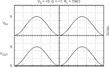 Figure 23. Rail-to-Rail Input and Output
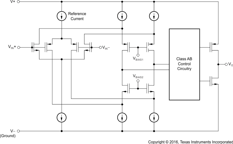
7.2 Functional Block Diagram
7.3 Feature Description
7.3.1 Operating Voltage
The OPA340 series operational amplifiers are fully specified from 2.7 V to 5 V. However, supply voltage may range from 2.5 V to 5.5 V. Parameters are ensured over the specified supply range—a unique feature of the OPA340 series. In addition, many specifications apply from –40°C to 85°C. Most behavior remains virtually unchanged throughout the full operating voltage range. Parameters which vary significantly with operating voltages or temperature are shown in the Typical Characteristics.
7.3.2 Rail-to-Rail Input
The input common-mode voltage range of the OPA340 series extends 500 mV beyond the supply rails. This extended range is achieved with a complementary input stage—an N-channel input differential pair in parallel with a P-channel differential pair. The N-channel pair is active for input voltages close to the positive rail, typically (V+) – 1.3 V to 500 mV above the positive supply, while the P-channel pair is on for inputs from 500 mV below the negative supply to approximately (V+) – 1.3 V. There is a small transition region, typically (V+) – 1.5 V to (V+) – 1.1 V, in which both pairs are on. This 400-mV transition region can vary ±300 mV with process variation. Thus, the transition region (both stages on) can range from (V+) – 1.8 V to (V+) – 1.4 V on the low end, up to (V+) – 1.2 V to (V+) – 0.8 V on the high end.
OPA340 series operational amplifiers are laser-trimmed to the reduce offset voltage difference between the N-channel and P-channel input stages, resulting in improved common-mode rejection and a smooth transition between the N-channel pair and the P-channel pair. However, within the 400-mV transition region PSRR, CMRR, offset voltage, offset drift, and THD may be degraded compared to operation outside this region.
A double-folded cascode adds the signal from the two input pairs and presents a differential signal to the class AB output stage. Normally, input bias current is approximately 200 fA; however, input voltages exceeding the power supplies by more than 500 mV can cause excessive current to flow in or out of the input pins. Momentary voltages greater than 500 mV beyond the power supply can be tolerated if the current on the input pins is limited to 10 mA. This current limiting is easily accomplished with an input resistor, as shown in Figure 24. Many input signals are inherently current-limited to less than 10 mA; therefore, a limiting resistor is not required.
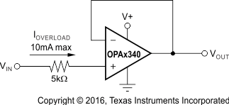 Figure 24. Input Current Protection for Voltages Exceeding the Supply Voltage
7.3.3 Rail-to-Rail Output
A class AB output stage with common-source transistors is used to achieve rail-to-rail output. For light resistive loads (> 50 kΩ), the output voltage is typically a few millivolts from the supply rails. With moderate resistive loads (2 kΩ to 50 kΩ), the output can swing to within a few tens of millivolts from the supply rails and maintain high open-loop gain (see Figure 15).
7.3.4 Capacitive Load and Stability
OPA340 series operational amplifiers can drive a wide range of capacitive loads. However, all operational amplifiers under certain conditions can become unstable. operational amplifier configuration, gain, and load value are some of the factors to consider when determining stability. An operational amplifier in unity-gain configuration is most susceptible to the effects of capacitive load. The capacitive load reacts with the output resistance of the operational amplifier, along with any additional load resistance, to create a pole in the small-signal response that degrades the phase margin. In unity-gain configuration, the OPA340 series operational amplifiers perform well, with a pure capacitive load up to approximately 1000 pF. Increasing gain enhances the amplifier ability to drive more capacitance (see Figure 21).
One method of improving capacitive load drive in the unity-gain configuration is to insert a 10-Ω to 20-Ω resistor in series with the output, as shown in Figure 25. This resistor significantly reduces ringing with large capacitive loads. However, if there is a resistive load in parallel with the capacitive load, it creates a voltage divider introducing a DC error at the output and slightly reduces output swing. This error can be insignificant. For instance, with RL = 10 kΩ and RS = 20 Ω, there is only an approximate 0.2% error at the output.
When used with the miniature package options of the OPA340 series, the combination is ideal for space-limited and low-power applications. For further information, consult the ADS7816 data sheet, 12-Bit High Speed Micro Power Sampling Analog-To-Digital Converter (SBAS061). With the OPA340 in a noninverting configuration, an RC network at the output of the amplifier can be used to filter high-frequency noise in the signal (see Figure 26). In the inverting configuration, filtering may be accomplished with a capacitor across the feedback resistor (see Figure 27).
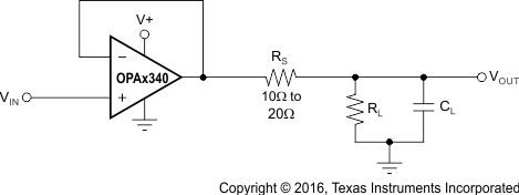 Figure 25. Series Resistor in Unity-Gain Configuration Improves Capacitive Load Drive
7.3.5 Driving A/D Converters
The OPA340 series operational amplifiers are optimized for driving medium-speed (up to 100 kHz) sampling A/D converters. However, they also offer excellent performance for higher speed converters. The OPA340 series provides an effective means of buffering the converter input capacitance and resulting charge injection while providing signal gain. Figure 26 and Figure 27 show the OPA340 driving an ADS7816. The ADS7816 is a 12-bit, micro-power sampling converter in the tiny 8-pin VSSOP package.
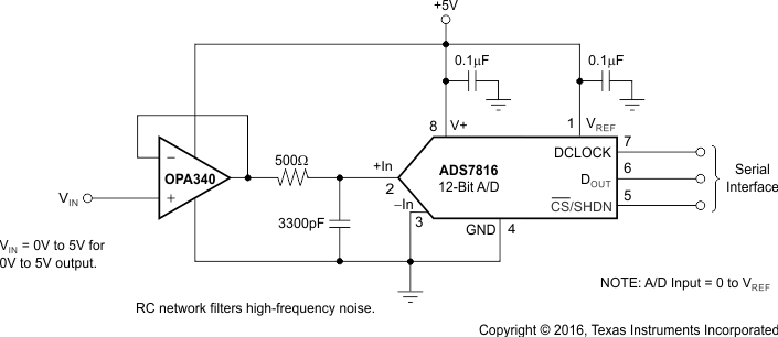 Figure 26. OPA340 in Noninverting Configuration Driving ADS7816
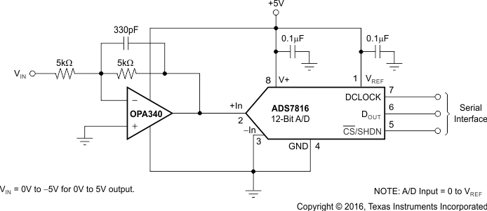 Figure 27. OPA340 in Inverting Configuration Driving ADS7816
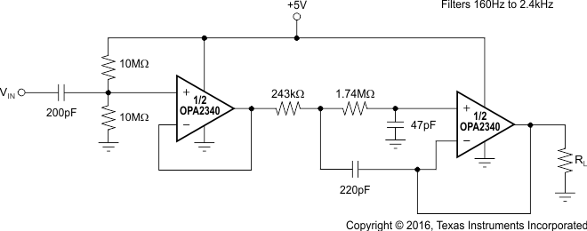 Figure 28. Speech Bandpass Filter
7.4 Device Functional Modes
The OPAx340 has a single functional mode and is operational when the power-supply voltage is greater than 2.7 V (±1.35 V). The maximum power supply voltage for the OPAx340 is 5.5 V (±2.75 V).