ZHCSKG0J October   2019  – April 2021 OPA2607 , OPA607

PRODUCTION DATA  

  1. 特性
  2. 应用
  3. 说明
  4. Revision History
  5. Device Comparison
  6. Pin Configuration and Functions
  7. Specifications
    1. 7.1 Absolute Maximum Ratings
    2. 7.2 ESD Ratings
    3. 7.3 Recommended Operating Conditions
    4. 7.4 Thermal Information
    5. 7.5 Electrical Characteristics
    6. 7.6 Typical Characteristics
  8. Detailed Description
    1. 8.1 Overview
    2. 8.2 Functional Block Diagram
    3. 8.3 Feature Description
      1. 8.3.1 Operating Voltage
      2. 8.3.2 Rail-to-Rail Output and Driving Capacitive Loads
      3. 8.3.3 Input and ESD Protection
      4. 8.3.4 Decompensated Architecture with Wide Gain-Bandwidth Product
    4. 8.4 Device Functional Modes
      1. 8.4.1 Normal Operating Mode
      2. 8.4.2 Power Down Mode
  9. Application and Implementation
    1. 9.1 Application Information
    2. 9.2 Typical Applications
      1. 9.2.1 100-kΩ Gain Transimpedance Design
        1. 9.2.1.1 Design Requirements
        2. 9.2.1.2 Detailed Design Procedure
        3. 9.2.1.3 Application Curves
      2. 9.2.2 Noninverting Gain of 3 V/V
      3. 9.2.3 High-Input Impedance (Hi-Z), High-Gain Signal Front-End
        1. 9.2.3.1 Design Requirements
        2. 9.2.3.2 Detailed Design Procedure
        3. 9.2.3.3 Application Curves
      4. 9.2.4 Low-Cost, Low Side, High-Speed Current Sensing
        1. 9.2.4.1 Design Requirements
        2. 9.2.4.2 Detailed Design Procedure
        3. 9.2.4.3 Application Curves
      5. 9.2.5 Ultrasonic Flow Meters
        1. 9.2.5.1 Design Requirements
  10. 10Power Supply Recommendations
  11. 11Layout
    1. 11.1 Layout Guidelines
    2. 11.2 Layout Examples
  12. 12Device and Documentation Support
    1. 12.1 Device Support
      1. 12.1.1 Development Support
    2. 12.2 Documentation Support
      1. 12.2.1 Related Documentation
    3. 12.3 Related Links
    4. 12.4 Receiving Notification of Documentation Updates
    5. 12.5 支持资源
    6. 12.6 Trademarks
    7. 12.7 Electrostatic Discharge Caution
    8. 12.8 Glossary
  13. 13Mechanical, Packaging, and Orderable Information

封装选项

机械数据 (封装 | 引脚)
散热焊盘机械数据 (封装 | 引脚)
订购信息

Rail-to-Rail Output and Driving Capacitive Loads

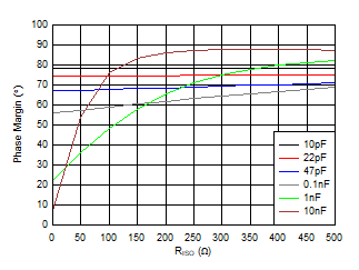
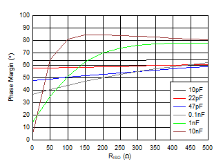
Designed as a low-power, low-voltage operational amplifier, the OPAx607 devices are capable of delivering a robust output drive. For resistive loads of 10 kΩ, the output swings to within a few millivolts of either supply rail, regardless of the applied power-supply voltage. Different load conditions change the ability of the amplifier to swing close to the rails. The OPAx607 devices drive up to a nominal capacitive load of 47 pF on the output with no special consideration and without the need of a series isolation resistor RISO while still being able to achieve 45° of phase margin. When driving capacitive loads greater than 47 pF, TI recommends using RISO as shown in Figure 8-1 in series with the output as close to the device as possible. Refer to Figure 7-18 for looking up different values of RISO required for CL to achieve 45° phase margin. Without RISO, the external capacitance (CL) interacts with the output impedance (ZO) of the amplifier, resulting in stability issues. Inserting RISO isolates CL from ZO and restores the phase margin. Figure 8-1 shows the test circuit.
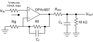
GUID-36EF99AD-46C4-45CA-B116-4685CCBCAE08-low.gifFigure 8-1 Input Current Protection and Driving Capacitive Loads

Figure 8-2 and Figure 8-3 show the phase margin achieved with varying RISO with different values of CL.
GUID-A42922A5-7F0B-4435-89D5-5BAB86073C63-low.gif
Gain = 10 V/V,Cf = 2.5 pF,RL = 10 kΩ
Figure 8-2 Phase Margin vs. Series Isolation Resistor
GUID-58CC1CD2-D558-45E6-8D39-23FB207FD416-low.gif
Gain = 20 V/V,Cf = 2.5 pF,RL = 10 kΩ
Figure 8-3 Phase Margin vs. Series Isolation Resistor