ZHCS959D June 2012 – September 2016 OPA4188
PRODUCTION DATA.
- 1 特性
- 2 应用范围
- 3 说明
- 4 修订历史记录
- 5 Zero-Drift Amplifier Portfolio
- 6 Pin Configuration and Functions
-
7 Specifications
- 7.1 Absolute Maximum Ratings
- 7.2 ESD Ratings
- 7.3 Recommended Operating Conditions
- 7.4 Thermal Information
- 7.5 Electrical Characteristics: High-Voltage Operation, VS = ±4 V to ±18 V (VS = 8 V to 36 V)
- 7.6 Electrical Characteristics: Low-Voltage Operation, VS = ±2 V to < ±4 V (VS = +4 V to < +8 V)
- 7.7 Typical Characteristics
- 8 Detailed Description
- 9 Applications and Implementation
- 10Power Supply Recommendations
- 11Layout
- 12器件和文档支持
- 13机械、封装和可订购信息
9 Applications and Implementation
NOTE
Information in the following applications sections is not part of the TI component specification, and TI does not warrant its accuracy or completeness. TI’s customers are responsible for determining suitability of components for their purposes. Customers should validate and test their design implementation to confirm system functionality.
9.1 Application Information
The OPA4188 operational amplifier combines precision offset and drift with excellent overall performance, making it ideal for many precision applications. The precision offset drift of only 0.085 µV per degree Celsius provides stability over the entire temperature range. In addition, the device offers excellent overall performance with high CMRR, PSRR, and AOL. As with all amplifiers, applications with noisy or high-impedance power supplies require decoupling capacitors close to the device pins. In most cases, 0.1-µF capacitors are adequate.
The application examples of Figure 46 and Figure 47 highlight only a few of the circuits where the OPA4188 device can be used.
9.1.1 Operating Characteristics
The OPA4188 device is specified for operation from 4 V to 36 V (±2 V to ±18 V). Many of the specifications apply from –40°C to 125°C. Parameters that can exhibit significant variance with regard to operating voltage or temperature are presented in the Typical Characteristics.
9.2 Typical Applications
9.2.1 Second Order Low Pass Filter
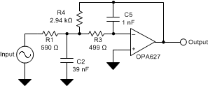
Low pass filters are commonly employed in signal processing applications to reduce noise and prevent aliasing. The OPA4188 device is ideally suited to construct a high precision active filter. Figure 44 illustrates a second order low pass filter commonly encountered in signal processing applications.
 Figure 44. 25-kHz Low Pass Filter
9.2.1.1 Design Requirements
Use the following parameters for this design example:
- Gain = 5 V/V (inverting gain)
- Low-pass cutoff frequency = 25 kHz
- Second order Chebyshev filter response with 3-dB gain peaking in the passband
9.2.1.2 Detailed Design Procedure
The infinite-gain multiple-feedback circuit for a low-pass network function is shown in Figure 44. Use Equation 1 to calculate the voltage transfer function.

This circuit produces a signal inversion. For this circuit, use Equation 2 to calculate the gain at DC and the low-pass cutoff frequency.

Software tools are readily available to simplify filter design. WEBENCH® Filter Designer is a simple, powerful, and easy-to-use active filter design program. The WEBENCH Filter Designer lets you create optimized filter designs using a selection of TI operational amplifiers and passive components from TI's vendor partners. Available as a web based tool from the WEBENCH® Design Center, WEBENCH® Filter Designer allows you to design, optimize, and simulate complete multi-stage active filter solutions within minutes.
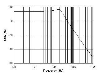
9.2.1.3 Application Curve
 Figure 45. Gain (dB) vs Frequency (Hz)
9.2.2 Discrete INA + Attenuation for ADC With a 3.3-V Supply
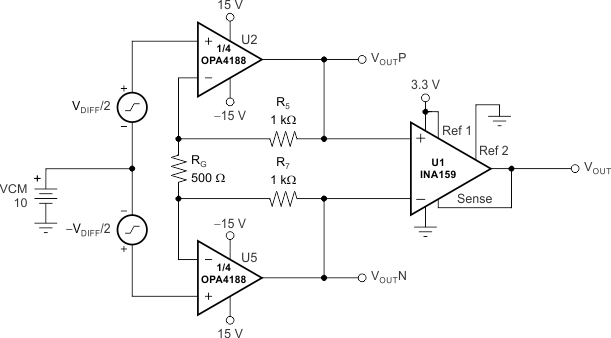
Figure 46 illustrates a circuit with high input impedance that can accommodate ±2 V differential input signals. The output, VOUT, is scaled into the full scale input range of a 3.3 V analog to digital converter. Input common mode voltages as high as ±10 V can be present with no signal clipping. Input stage gain is determined by resistors R5, RG and R7 according to Equation 3 .

 Figure 46. Discrete INA + Attenuation for ADC With a 3.3-V Supply Circuit
9.2.3 RTD Amplifier With Linearization
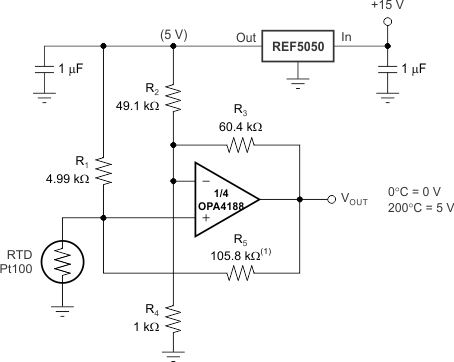
The OPA4188 device with ultra-low input offset voltage and ultra-low input offset voltage drift is ideally suited for RTD signal conditioning. Figure 47 illustrates a Pt100 RTD with excitation provided by a voltage reference and resistor R1. Linearization is provided by R5. Gain is determined by R2, R3 and R4. The circuit is configured such that the output, VOUT, ranges from 0 V to 5 V over the temperature range from 0°C to 200°C. The OPA4188 requires split power supplies (±5.35 V to ±15 V) for proper operation in this configuration.
