ZHCSGP3D September   2017  – December 2018 OPA2837 , OPA837

PRODUCTION DATA.  

  1. 特性
  2. 应用
    1.     具有真正接地输入和输出范围的低功耗、低噪声、精密单端 SAR ADC 驱动器
  3. 说明
    1.     Device Images
  4. 修订历史记录
  5. Pin Configuration and Functions
    1.     Pin Functions
  6. Specifications
    1. 6.1  Absolute Maximum Ratings
    2. 6.2  ESD Ratings
    3. 6.3  Recommended Operating Conditions
    4. 6.4  Thermal Information: OPA837
    5. 6.5  Thermal Information: OPA2837
    6. 6.6  Electrical Characteristics: VS = 5 V
    7. 6.7  Electrical Characteristics: VS = 3 V
    8. 6.8  Typical Characteristics: VS = 5.0 V
    9. 6.9  Typical Characteristics: VS = 3.0 V
    10. 6.10 Typical Characteristics: ±2.5-V to ±1.5-V Split Supply
  7. Detailed Description
    1. 7.1 Overview
    2. 7.2 Functional Block Diagrams
    3. 7.3 Feature Description
      1. 7.3.1 OPA837 Comparison
      2. 7.3.2 Input Common-Mode Voltage Range
      3. 7.3.3 Output Voltage Range
      4. 7.3.4 Power-Down Operation
      5. 7.3.5 Low-Power Applications and the Effects of Resistor Values on Bandwidth
      6. 7.3.6 Driving Capacitive Loads
    4. 7.4 Device Functional Modes
      1. 7.4.1 Split-Supply Operation (±1.35 V to ±2.7 V)
      2. 7.4.2 Single-Supply Operation (2.7 V to 5.4 V)
  8. Application and Implementation
    1. 8.1 Application Information
      1. 8.1.1  Noninverting Amplifier
      2. 8.1.2  Inverting Amplifier
      3. 8.1.3  Output DC Error Calculations
      4. 8.1.4  Output Noise Calculations
      5. 8.1.5  Instrumentation Amplifier
      6. 8.1.6  Attenuators
      7. 8.1.7  Differential to Single-Ended Amplifier
      8. 8.1.8  Differential-to-Differential Amplifier
      9. 8.1.9  Pulse Application With Single-Supply Circuit
      10. 8.1.10 ADC Driver Performance
    2. 8.2 Typical Applications
      1. 8.2.1 Active Filters
        1. 8.2.1.1 Design Requirements
        2. 8.2.1.2 Detailed Design Procedure
        3. 8.2.1.3 Application Curves
      2. 8.2.2 Implementing a 2:1 Active Multiplexer
        1. 8.2.2.1 Design Requirements
        2. 8.2.2.2 Detailed Design Procedure
      3. 8.2.3 1-Bit PGA Operation
        1. 8.2.3.1 Design Requirements
        2. 8.2.3.2 Detailed Design Procedure
  9. Power Supply Recommendations
  10. 10Layout
    1. 10.1 Layout Guidelines
    2. 10.2 Layout Example
  11. 11器件和文档支持
    1. 11.1 文档支持
      1. 11.1.1 相关文档
    2. 11.2 相关链接
    3. 11.3 接收文档更新通知
    4. 11.4 社区资源
    5. 11.5 商标
    6. 11.6 静电放电警告
    7. 11.7 术语表
  12. 12机械、封装和可订购信息

封装选项

机械数据 (封装 | 引脚)
散热焊盘机械数据 (封装 | 引脚)
订购信息

Typical Characteristics: VS = 3.0 V

at VS+ = 3.0 V, VS– = 0 V, VOUT = 1 VPP, RF = 0 Ω, RL = 2 kΩ, G = 1 V/V, input and output referenced to mid-supply, and TA ≈ 25°C (unless otherwise noted)
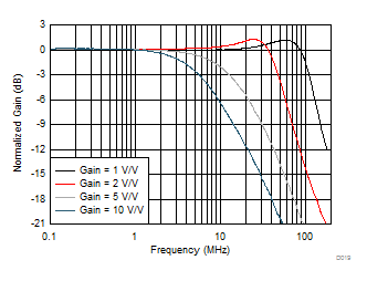
OPA837 OPA2837 D019_SBOS673.gif
See Figure 74 and Table 2, VOUT = 20 mVPP, RLOAD = 2 kΩ
Figure 19. Noninverting Small-Signal Response vs Gain
OPA837 OPA2837 D021_SBOS673.gif
See Figure 74, gain = 2 V/V
Figure 21. Noninverting Large-Signal Bandwidth vs VOPP
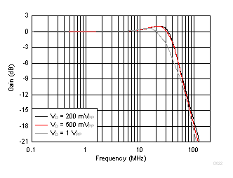
OPA837 OPA2837 D023_SBOS673.gif
See Figure 74 and Table 2, VOUT = 200 mVPP, RLOAD = 2 kΩ
Figure 23. Noninverting Response Flatness vs Gain
OPA837 OPA2837 D025_SBOS673.gif
See Figure 74 and Table 2, gain = 2 V/V,
input edge rate set to stay below slew limiting
Figure 25. Noninverting Step Response vs VOPP
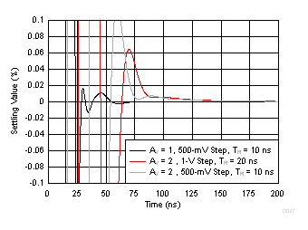
OPA837 OPA2837 D027_SBOS673.gif
See Figure 74 and Table 2
Figure 27. Simulated Noninverting Settling Time
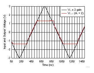
OPA837 OPA2837 D029_SBOS673.gif
See Figure 74 and Table 2, gain = 2 V/V
Figure 29. Noninverting Overdrive Recovery
OPA837 OPA2837 D031_SBOS673.gif
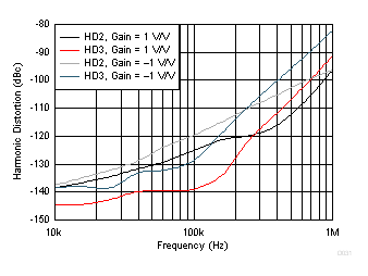
See Figure 74, Figure 75, Table 2, and Table 3, VOUT = 1 VPP, RLOAD = 2 kΩ
Figure 31. Harmonic Distortion vs Frequency
OPA837 OPA2837 D033_SBOS673.gif
See Figure 74, Figure 75, Table 2, and Table 3, RLOAD = 2 kΩ,
f = 100 kHz
Figure 33. Harmonic Distortion vs Output Swing
OPA837 OPA2837 D035_SBOS673.gif
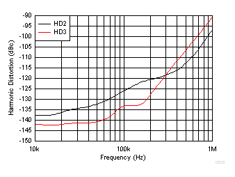
See Figure 87, gain = 1 V/V, VOUT = 1 VPP, RLOAD = 2 kΩ
Figure 35. Harmonic Distortion as Active Mux
OPA837 OPA2837 D020_SBOS673.gif
See Figure 75 and Table 3, VOUT = 20 mVPP, RLOAD = 2 kΩ
Figure 20. Inverting Small-Signal Response vs Gain
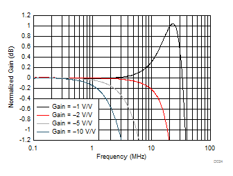
OPA837 OPA2837 D022_SBOS673.gif
See Figure 75, gain = –1 V/V
Figure 22. Inverting Large-Signal Bandwidth vs VOPP
OPA837 OPA2837 D024_SBOS673.gif
See Figure 75 and Table 3, VOUT = 200 mVPP, RLOAD = 2 kΩ
Figure 24. Inverting Response Flatness vs Gain
OPA837 OPA2837 D026_SBOS673.gif
See Figure 75 and Table 3, gain = –1 V/V,
input edge rate set to stay below slew limiting
Figure 26. Inverting Step Response vs VOPP
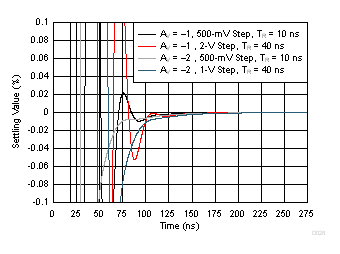
OPA837 OPA2837 D028_SBOS673.gif
See Figure 75 and Table 3
Figure 28. Simulated Inverting Settling Time
OPA837 OPA2837 D030_SBOS673.gif
See Figure 75 and Table 3, gain = –1 V/V
Figure 30. Inverting Overdrive Recovery
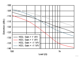
OPA837 OPA2837 D032_SBOS673.gif
See Figure 74, Figure 75, Table 2, and Table 3, VOUT = 1 VPP,
f = 100 kHz, RLOAD = 2 kΩ
Figure 32. Harmonic Distortion vs RLOAD
OPA837 OPA2837 D034_SBOS673.gif
See Figure 74, Figure 75, Table 2, and Table 3, RLOAD = 2 kΩ,
f = 100 kHz, VOUT = 1 VPP
Figure 34. Harmonic Distortion vs Gain Magnitude
OPA837 OPA2837 D036_SBOS673.gif
See Figure 88, gain of 1 V/V and 2 V/V, VOUT = 1 VPP,
RLOAD = 2 kΩ
Figure 36. Harmonic Distortion as 1-Bit PGA