ZHCSGP3D September 2017 – December 2018 OPA2837 , OPA837
PRODUCTION DATA.
- 1 特性
- 2 应用
- 3 说明
- 4 修订历史记录
- 5 Pin Configuration and Functions
-
6 Specifications
- 6.1 Absolute Maximum Ratings
- 6.2 ESD Ratings
- 6.3 Recommended Operating Conditions
- 6.4 Thermal Information: OPA837
- 6.5 Thermal Information: OPA2837
- 6.6 Electrical Characteristics: VS = 5 V
- 6.7 Electrical Characteristics: VS = 3 V
- 6.8 Typical Characteristics: VS = 5.0 V
- 6.9 Typical Characteristics: VS = 3.0 V
- 6.10 Typical Characteristics: ±2.5-V to ±1.5-V Split Supply
- 7 Detailed Description
-
8 Application and Implementation
- 8.1
Application Information
- 8.1.1 Noninverting Amplifier
- 8.1.2 Inverting Amplifier
- 8.1.3 Output DC Error Calculations
- 8.1.4 Output Noise Calculations
- 8.1.5 Instrumentation Amplifier
- 8.1.6 Attenuators
- 8.1.7 Differential to Single-Ended Amplifier
- 8.1.8 Differential-to-Differential Amplifier
- 8.1.9 Pulse Application With Single-Supply Circuit
- 8.1.10 ADC Driver Performance
- 8.2 Typical Applications
- 8.1
Application Information
- 9 Power Supply Recommendations
- 10Layout
- 11器件和文档支持
- 12机械、封装和可订购信息
8.2.2 Implementing a 2:1 Active Multiplexer
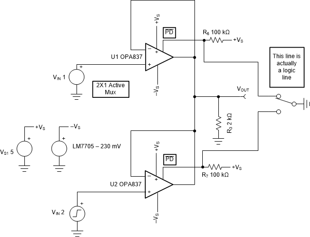
The OPA837 includes a unique feature that enables a much improved wired-or mux operation. When disabled, an internal switch opens from the inverting input to the active transistors isolating those nonlinear loads from the signal being driven back into the inverting input through the active channel. Figure 87 illustrates a simple example of this multiplexer. In this figure, one of two signals are selected to be passed on to a shared output. The logic control turns both amplifiers off (logic low) prior to turning one of them on. This control eliminates both outputs being active at the same time. If both amplifiers must be on, as in the simple switch illustrated in Figure 87, adding 100-Ω isolating resistors inside the loop at the outputs limits the current flow when both amplifiers are turned on. This solution offers a very high input impedance to both inputs, very low buffered output drive, and nearly perfect channel-to-channel isolation. The example of Figure 87 also includes a –0.23-V supply generator to allow true swing to ground on the output pins. This negative supply generator is optional if the outputs are more than 0.1 V above ground or intended to be AC-coupled. Testing with a single channel active and an off channel attached to the output showed no degradation in harmonic distortion; see Figure 17 and Figure 35. This approach can be expanded to more than two channels or to operate with gain in the channels. Adding more than two select channels in parallel should add 100-Ω feedback resistors to isolate the inverting input capacitance from the active output channel.
 Figure 87. 2:1 Active Multiplexer