ZHCSM22 October 2020 OPA856
PRODUCTION DATA
8.3.3 Wide Gain-Bandwidth Product
Figure 7-7 shows the open-loop magnitude and phase response of the OPA856. Calculate the gain bandwidth product of any op amp by determining the frequency at which the AOL is 40 dB and multiplying that frequency by a factor of 100. The open-loop response shows the OPA856 to have approximately 57° of phase-margin when configured as a unity-gain buffer.
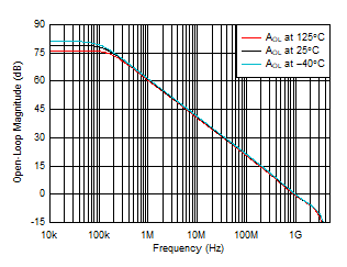
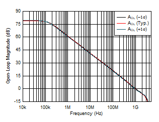
Figure 8-5 shows the open-loop magnitude (AOL) of the OPA856 as a function of temperature. The results show minimal variation over the entire temperature range. Semiconductor process variation is the naturally occurring variation in the attributes of a transistor (Early-voltage, β, channel-length, and width) and other passive elements (resistors and capacitors) when fabricated into an integrated circuit. The process variation can occur across devices on a single wafer or across devices over multiple wafer lots over time. Typically the variation across a single wafer is tightly controlled. Figure 8-6 shows the AOL magnitude of the OPA856 as a function of process variation over time. The results show the AOL curve for the nominal process corner and the variation one standard deviation from the nominal. The simulated results show less than 5° of phase-margin difference within a standard deviation of process variation when the amplifier is configured as a unity-gain bufffer.
 Figure 8-5 Open-Loop Gain vs Temperature
 Figure 8-6 Open-Loop Gain vs Process Variation