ZHCSFL9 October 2016 OPT3006
PRODUCTION DATA.
- 1 特性
- 2 应用
- 3 说明
- 4 修订历史记录
- 5 Pin Configuration and Functions
- 6 Specifications
-
7 Detailed Description
- 7.1 Overview
- 7.2 Functional Block Diagram
- 7.3 Feature Description
- 7.4 Device Functional Modes
- 7.5 Programming
- 7.6
Register Maps
- 7.6.1
Internal Registers
- 7.6.1.1
Register Descriptions
- 7.6.1.1.1 Result Register (offset = 00h)
- 7.6.1.1.2 Configuration Register (offset = 01h) [reset = C810h]
- 7.6.1.1.3 Low-Limit Register (offset = 02h) [reset = C0000h]
- 7.6.1.1.4 High-Limit Register (offset = 03h) [reset = BFFFh]
- 7.6.1.1.5 Manufacturer ID Register (offset = 7Eh) [reset = 5449h]
- 7.6.1.1.6 Device ID Register (offset = 7Fh) [reset = 3001h]
- 7.6.1.1
Register Descriptions
- 7.6.1
Internal Registers
- 8 Application and Implementation
- 9 Power-Supply Recommendations
- 10Layout
- 11器件和文档支持
- 12机械、封装和可订购信息
8 Application and Implementation
NOTE
Information in the following applications sections is not part of the TI component specification, and TI does not warrant its accuracy or completeness. TI’s customers are responsible for determining suitability of components for their purposes. Customers should validate and test their design implementation to confirm system functionality.
8.1 Application Information
Ambient light sensors are used in a wide variety of applications that require control as a function of ambient light. Because ambient light sensors nominally match the human eye spectral response, they are superior to photodiodes when the goal is to create an experience for human beings. Very common applications include display optical-intensity control and industrial or home lighting control.
There are two categories of interface to the OPT3006: electrical and optical.
8.1.1 Electrical Interface
The electrical interface is quite simple, as illustrated in Figure 29. Connect the OPT3006 I2C SDA and SCL pins to the same pins of an applications processor, microcontroller, or other digital processor. If that digital processor requires an interrupt resulting from an event of interest from the OPT3006, then connect the INT pin to either an interrupt or general-purpose I/O pin of the processor. There are multiple uses for this interrupt, including signaling the system to wake up from low-power mode, processing other tasks while waiting for an ambient light event of interest, or alerting the processor that a sample is ready to be read. Connect pullup resistors between a power supply appropriate for digital communication and the SDA and SCL pins (because they have open-drain output structures). If the INT pin is used, connect a pullup resistor to the INT pin. A typical value for these pullup resistors is 10 kΩ. The resistor choice can be optimized in conjunction to the bus capacitance to balance the system speed, power, noise immunity, and other requirements.
The power supply and grounding considerations are discussed in the Power-Supply Recommendations section.
Although spike suppression is integrated in the SDA and SCL pin circuits, use proper layout practices to minimize the amount of coupling into the communication lines. One possible introduction of noise occurs from capacitively coupling signal edges between the two communication lines themselves. Another possible noise introduction comes from other switching noise sources present in the system, especially for long communication lines. In noisy environments, shield communication lines to reduce the possibility of unintended noise coupling into the digital I/O lines that could be incorrectly interpreted.
8.1.2 Optical Interface
The optical interface is physically located on the same side of the device as the electrical interface, as shown in the Sensing Area of the mechanical packages at the end of this data sheet. At a system level, this configuration requires that the light that illuminates the sensor must come through the PCB or FPCB. Typically, the best solution is to create a cutout area in the PCB. Other solutions are possible, but with associated design trade-offs. This cutout must be carefully designed because the dimensions and tolerances impact the net-system, optical field-of-view performance. The design of this cutout is discussed more in the Design Requirements section.
Physical components, such as a plastic housing and a window that allows light from outside of the design to illuminate the sensor (see Figure 30), can help protect the OPT3006 and neighboring circuitry. Sometimes, a dark or opaque window is used to further enhance the visual appeal of the design by hiding the sensor from view. This window material is typically transparent plastic or glass.
Any physical component that affects the light that illuminates the sensing area of a light sensor also affects the performance of that light sensor. Therefore, for optimal performance, make sure to understand and control the effect of these components. Design a window width and height to permit light from a sufficient field of view to illuminate the sensor. For best performance, use a field of view of at least ±35°, or ideally ±45° or more. Understanding and designing the field of view is discussed further in application report SBEA002, OPT3001: Ambient Light Sensor Application Guide.
The visible-spectrum transmission for dark windows typically ranges between 5% to 30%, but can be less than 1%. Specify a visible-spectrum transmission as low as, but no more than, necessary to achieve sufficient visual appeal because decreased transmission decreases the available light for the sensor to measure. The windows are made dark by either applying an ink to a transparent window material, or including a dye or other optical substance within the window material itself. This attenuating transmission in the visible spectrum of the window creates a ratio between the light on the outside of the design and the light that is measured by the OPT3006. To accurately measure the light outside of the design, compensate the OPT3006 measurement for this ratio.
Ambient light sensors are used to help create ideal lighting experiences for humans; therefore, the matching of the sensor spectral response to that of the human eye response is vital. Infrared light is not visible to the human eye, and can interfere with the measurement of visible light when sensors lack infrared rejection. Therefore, the ratio of visible light to interfering infrared light affects the accuracy of any practical system that represents the human eye. The strong rejection of infrared light by the OPT3006 allows measurements consistent with human perception under high-infrared lighting conditions, such as from incandescent, halogen, or sunlight sources.
Although the inks and dyes of dark windows serve their primary purpose of being minimally transmissive to visible light, some inks and dyes can also be very transmissive to infrared light. The use of these inks and dyes further decreases the ratio of visible to infrared light, and thus decreases sensor measurement accuracy. However, because of the excellent infrared rejection of the OPT3006, this effect is minimized, and good results are achieved under a dark window with similar spectral responses to those shown in Figure 32.
For best accuracy, avoid grill-like window structures, unless the designer understands the optical effects sufficiently. These grill-like window structures create a nonuniform illumination pattern at the sensor that make light measurement results vary with placement tolerances and angle of incidence of the light. If a grill-like structure is desired, the OPT3006 is an excellent sensor choice because it is minimally sensitive to illumination uniformity issues disrupting the measurement process.
Light pipes can appear attractive for aiding in the optomechanical design that brings light to the sensor; however, do not use light pipes with any ambient light sensor unless the system designer fully understands the ramifications of the optical physics of light pipes within the full context of his design and objectives.
8.2 Typical Application
Measuring the ambient light with the OPT3006 mounted on a flexible printed circuit board (FPCB) is described in this section. The schematic for this design is shown in Figure 29.
 Figure 29. Measuring Ambient Light on an FPCB
8.2.1 Design Requirements
This design focuses on the field of view, or angular response, of an OPT3006 mounted on an FPCB with an area cut out that permits light to illuminate the sensor. As a result of the geometry of this cutout, the system field of view (angular response) depends on the axis of rotation. One axis of rotation has a less restricted field of view, and the other axis of rotation has a more restricted field of view. The basic requirements of this design are:
- Mount the OPT3006 onto an FPCB with a cutout that allows light to illuminate the sensor.
- The field of view along the axis of rotation with the less restricted field of view must match the device performance.
- The field of view for the more restricted axis of rotation must be minimum of ±30°.
Field of view is traditionally defined as the angle at which the angular response is 50% of the maximum value of the system response.
8.2.2 Detailed Design Procedure
8.2.2.1 Optomechanical Design
After completing the electrical design (see Figure 29), the next task is the optomechanical design of the FPCB cutout. Design this cutout in conjunction with the tolerance capabilities of the FPCB manufacturer. Or, conversely, choose the FPCB manufacturer for its capabilities of optimally creating this cutout. A semi-rectangular shape of the cutout, created with a standard FPCB laser, is presented here. There are many alternate approaches with different cost, tolerance, and performance tradeoffs.
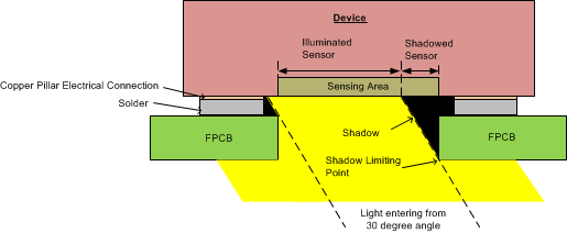
An image of the created FPCB with the rectangular cutout is shown in Figure 30. The long (vertical) direction of the cutout obviously has no effect on the angular response because any shadows created from the FPCB do not come near the sensor. The long cutout direction defines the axis of rotation with the less restricted field of view. The narrow (horizontal) direction of the cutout, which is limited by the electrical connections to OPT3006, can create shadows that can have a minor impact on the angular response. The narrow cutout direction defines the axis of rotation of the more restricted view. The possibility of shadows are illustrated in Figure 31, a cross-sectional diagram showing the OPT3006 device, with the sensing area, soldered to the FPCB with the cutout.
 Figure 30. Image of FPCB With OPT3006 Mounted, Receiving Light Through the Cutout
 Figure 31. Cross-Sectional Diagram of OPT3006 Soldered to an FPCB With a Cutout, Including Light Entering From an Angle
To design the angular response to have greater than 50% response at 30°, the optical mechanisms must be understood. This analysis is simplified by assuming a perfectly rectangular cutout. The concepts for this rectangular cutout apply to nonrectangular cutouts, but require a more complex 3D analysis. The analysis performed here is approximate because the actual cutout is not perfectly rectangular.
The net system response is the response of the device without the shadowing effect, multiplied by the percentage of the device that is illuminated, per Equation 5:
The shadow impacts the percentage of the sensor that can be illuminated, as seen in Figure 31. The percent response of a shadowed sensor is the percent of the sensor that is illuminated.
The percent of the sensor that must be illuminated to achieve > 50% response is derived by the sequence of Equation 6 through Equation 8.
The device has a 75% response at 30°, as shown in Figure 13, and is a little less than the expected cosine of 30°. The resulting device illumination is shown inEquation 9.
Hence, the 3-dimensional geometry illustrated in Figure 31 must permit greater than 66% of the sensor to be illuminated at a 30° angle of incident light. To quantify the geometry of this design, the post-SMT solder thickness is approximately 37 µm (half the thickness of the pre-SMT solder paste thickness), the copper pillar electrical connection is 7 µm, and the FPCB is 105 µm. Therefore, the shadow limiting point is 37 µm + 7 µm + 105 µm = 149 µm, higher than the sensing surface. The 30° angle shadow extends beyond that shadow limiting point per Equation 10.
For this instance of the design and tolerance, the shadow limiting point of FPCB cutout is roughly even with the sensor edge, so 86 µm of the sensor is under shadow. If the shadow limiting point was not even with the sensor edge because of either the design or the tolerances, an extra term is added per the system geometry. Given that the sensor width is 381 µm (per the attached mechanical drawing at the end of this data sheet), the amount of illuminated sensor is 381 µm – 86 µm = 295 µm = 77.4%.
The net response at the 30° angle is predicted byEquation 11
There might be an additional need to put a product casing over the assembly of OPT3006 and the FPCB. The window sizing and placement for such an assembly is discussed in more rigorous detail in application report OPT3001: Ambient Light Sensor Application Guide (SBEA002).
8.2.3 Application Curves
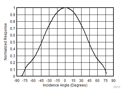
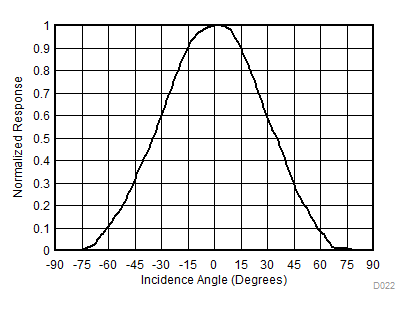
To validate the angular response of the design, put a light source in a fixed position, allow the device assembly to rotate, and take device measurements at a series of angles. The resulting angular response of this design along the less-restricted rotational axis is shown in Figure 32. The resulting angular response of the more-restricted rotational axis is shown in Figure 33. The response of the device at a 30° angle is approximately 60%, and is very close to the 58% predicted by Equation 11 in the preceding analysis.
 Figure 32. Angular Response of this FPCB Design Along the Less-Restricted Rotational Axis
 Figure 33. Angular Response of this FPCB Design Along the More-Restricted Rotational Axis
8.3 Do's and Don'ts
As with any optical product, take special care when handling the OPT3006. The OPT3006 is a piece of active silicon, without the mechanical protection of an epoxy-like package or other reenforcement. This design allows the device to be as thin as possible. Take extra care to handle the device gently in order to not crack or break the device. Use a properly-sized vacuum manipulation tool to handle the device.
Although the OPT3006 has low sensitivity to dust and scratches, proper optical device handling procedures are still required.
The optical surface of the device must be kept clean for optimal performance, both when prototyping with the device, and during mass production manufacturing procedures. Keep the optical surface clean of fingerprints, dust, and other optical-inhibiting contaminants.
If the optical surface of the device requires cleaning, use a few gentle brushes with a soft swab of deionized water or isopropyl alcohol. Avoid potentially abrasive cleaning and manipulating tools and excessive force that can scratch the optical surface.
If the OPT3006 performs less than optimally, inspect the optical surface for dirt, scratches, or other optical artifacts.