SLES248A May 2009 – March 2015 PCM1795
PRODUCTION DATA.
- 1 Features
- 2 Applications
- 3 Description
- 4 Revision History
- 5 Pin Configuration and Functions
- 6 Specifications
-
7 Detailed Description
- 7.1 Overview
- 7.2 Functional Block Diagram
- 7.3 Feature Description
- 7.4 Device Functional Modes
- 7.5 Programming
- 7.6
Register Maps
- 7.6.1
Mode Control Registers
- 7.6.1.1 User-Programmable Mode Controls
- 7.6.1.2 Register Map
- 7.6.1.3
Register Definitions
- 7.6.1.3.1 R/W: Read/Write Mode Select
- 7.6.1.3.2 ATx[7:0]: Digital Attenuation Level Setting
- 7.6.1.3.3 R/W: Read/Write Mode Select
- 7.6.1.3.4 ATLD: Attenuation Load Control
- 7.6.1.3.5 FMT[2:0]: Audio Interface Data Format
- 7.6.1.3.6 DMF[1:0]: Sampling Frequency Selection for the De-Emphasis Function
- 7.6.1.3.7 DME: Digital De-Emphasis Control
- 7.6.1.3.8 MUTE: Soft Mute Control
- 7.6.1.3.9 R/W: Read/Write Mode Select
- 7.6.1.3.10 REV: Output Phase Reversal
- 7.6.1.3.11 ATS[1:0]: Attenuation Rate Select
- 7.6.1.3.12 OPE: DAC Operation Control
- 7.6.1.3.13 DFMS: Stereo DF Bypass Mode Select
- 7.6.1.3.14 FLT: Digital Filter Roll-Off Control
- 7.6.1.3.15 INZD: Infinite Zero Detect Mute Control
- 7.6.1.3.16 R/W: Read/Write Mode Select
- 7.6.1.3.17 SRST: System Reset Control
- 7.6.1.3.18 DSD: DSD Interface Mode Control
- 7.6.1.3.19 DFTH: Digital Filter Bypass (or Through Mode) Control
- 7.6.1.3.20 MONO: Monaural Mode Selection
- 7.6.1.3.21 CHSL: Channel Selection for Monaural Mode
- 7.6.1.3.22 OS[1:0]: ΔΣ Oversampling Rate Selection
- 7.6.1.3.23 R/W: Read/Write Mode Select
- 7.6.1.3.24 DZ[1:0]: DSD Zero Output Enable
- 7.6.1.3.25 PCMZ: PCM Zero Output Enable
- 7.6.1.3.26 R: Read Mode Select
- 7.6.1.3.27 ZFGx: Zero-Detection Flag
- 7.6.1.3.28 Read Mode Select
- 7.6.1.3.29 ID[4:0]: Device ID
- 7.6.1
Mode Control Registers
-
8 Application and Implementation
- 8.1 Application Information
- 8.2
Typical Applications
- 8.2.1 Typical Connection Diagram in PCM Mode
- 8.2.2
Application for External Digital Filter Interface
- 8.2.2.1 Design Requirements
- 8.2.2.2 Detailed Design Procedure
- 8.2.2.3 Application Curves
- 8.2.3 Application for DSD Format (DSD Mode) Interface
- 8.2.4
TDMCA Interface Format
- 8.2.4.1 Design Requirements
- 8.2.4.2
Detailed Design Procedure
- 8.2.4.2.1 TDMCA Mode Determination
- 8.2.4.2.2 TDMCA Terminals
- 8.2.4.2.3 Device ID Determination
- 8.2.4.2.4 TDMCA Frame
- 8.2.4.2.5
Command Field
- 8.2.4.2.5.1 Bit 31: Device ID Enable Flag
- 8.2.4.2.5.2 Bit 30: Extended Command Enable Flag
- 8.2.4.2.5.3 Bit 29: Daisy-Chain Selection Flag
- 8.2.4.2.5.4 Bits[28:24]: Device ID
- 8.2.4.2.5.5 Bit 23: Command Read/Write flag
- 8.2.4.2.5.6 Bits[22:16]: Register ID
- 8.2.4.2.5.7 Bits[15:8]: Command data
- 8.2.4.2.5.8 Bits[7:0]: Not used
- 8.2.4.2.6 Extended Command Field
- 8.2.4.2.7 Audio Fields
- 8.2.4.2.8 TDMCA Register Requirements
- 8.2.4.2.9 Register Write/Read Operation
- 8.2.4.2.10 TDMCA Mode Operation
- 9 Power Supply Recommendations
- 10Layout
- 11Device and Documentation Support
- 12Mechanical, Packaging, and Orderable Information
8 Application and Implementation
NOTE
Information in the following applications sections is not part of the TI component specification, and TI does not warrant its accuracy or completeness. TI’s customers are responsible for determining suitability of components for their purposes. Customers should validate and test their design implementation to confirm system functionality.
8.1 Application Information
The PCM1795 device is a software-controlled, differential current output DAC that can accept multiple formats of 16-, 24-, or 32-bit PCM audio data, DSD audio data, or TDMCA data. Because the PCM1795 is a current output part, in most cases a current to voltage stage is required before the signal is passed to the amplifier stage. A microcontroller or DSP can use SPI or I2C to control the PCM1795 with ZEROL and ZEROR as status pins for the outputs. The PCM1795 requires a 5-V analog supply, as well as a 3.3-V digital supply.
8.2 Typical Applications
8.2.1 Typical Connection Diagram in PCM Mode
Figure 52 shows a typical application circuit for PCM mode operation.
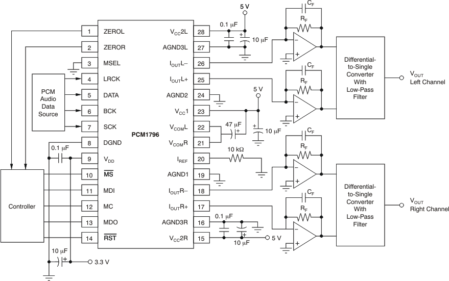 Figure 52. Typical Application Circuit for Standard PCM Audio Operation
8.2.1.1 Design Requirements
- Control: Host controller with SPI communication
- Audio Output: I/V output circuitry
- Audio Input: PCM, DSD, or TDMCA Digital Audio signal
8.2.1.2 Detailed Design Procedure
The design of the application circuit is very important in order to actually realize the high S/N ratio of which the PCM1795 device is capable, because noise and distortion that are generated in an application circuit are not negligible.
In the third-order, low-pass filter (LPF) circuit of Figure 53, the output level of 2.1 V RMS and 123-dB signal-to-noise ratio is achieved.
Figure 54 shows a circuit for the DSD mode, which is a fourth-order LPF in order to reduce the out-of-band noise.
8.2.1.2.1 I/V Section
The current of the PCM1795 device on each of the output pins (IOUTL+, IOUTL–, IOUTR+, IOUTR–) is 4 mAPP at 0 dB (full-scale). The voltage output level of the current-to-voltage (I/V) converter, VI, is given by Equation 2.
where
- RF = feedback resistance of the I/V converter
An NE5534 operational amplifier is recommended for the I/V circuit to obtain the specified performance. Dynamic performance such as the gain bandwidth, settling time, and slew rate of the operational amplifier affects the audio dynamic performance of the I/V section.
8.2.1.2.2 Differential Section
The PCM1795 device voltage outputs are followed by differential amplifier stages that sum the differential signals for each channel, creating a single-ended I/V op-amp output. In addition, the differential amplifiers provide a low-pass filter function.
The operational amplifier recommended for the differential circuit is the low-noise type.
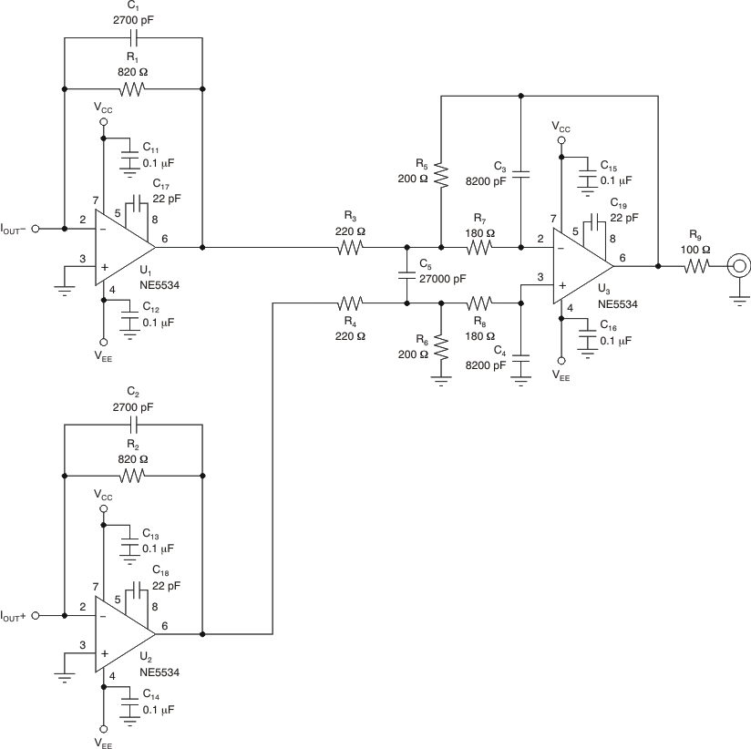 Figure 53. Measurement Circuit for PCM
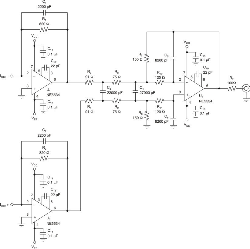 Figure 54. Measurement Circuit for DSD
8.2.1.3 Application Curves
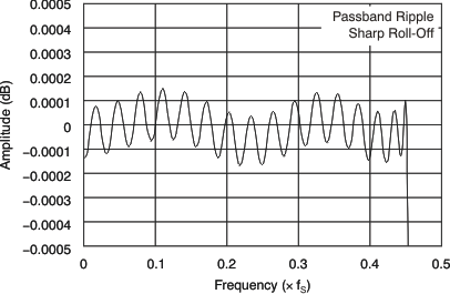 Figure 56. Amplitude vs Frequency
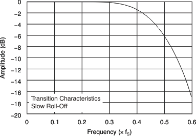 Figure 57. Amplitude vs Frequency
8.2.2 Application for External Digital Filter Interface
Figure 58 shows the connection diagram for an external digital filter.
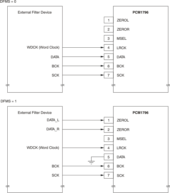 Figure 58. Connection Diagram for External Digital Filter (Internal DF Bypass Mode) Application
8.2.2.1 Design Requirements
- Control: Host controller with SPI communication
- Audio Output: I/V output circuitry
- Audio Input: Digital Audio Filter with I2S or DSD output
8.2.2.2 Detailed Design Procedure
8.2.2.2.1 Application for Interfacing With an External Digital Filter
For some applications, it may be desirable to use an external digital filter to perform the interpolation function, as it can provide improved stop-band attenuation when compared to the internal digital filter of the PCM1795 device.
The PCM1795 device supports several external digital filters, including:
- Texas Instruments DF1704 and DF1706
- Pacific Microsonics PMD200 HDCD filter/decoder IC
- Programmable DSPs
The external digital filter application mode is accessed by programming the following bits in the corresponding control register:
- DFTH = 1 (register 20)
The pins used to provide the serial interface for the external digital filter are illustrated in Figure 58. The word clock (WDCK) signal must be operated at 8 times or 4 times the desired sampling frequency, fS.
8.2.2.2.2 Pin Assignment When Using the External Digital Filter Interface
- LRCK (pin 4): WDCK as word clock input
- BCK (pin 6): Bit clock for audio data
- DATA (pin 5): Monaural audio data input when the DFMS bit is not set to 1
- ZEROL (pin 1): DATAL as left channel audio data input when the DFMS bit is set to 1
- ZEROR (pin 2): DATAR as right channel audio data input when the DFMS bit is set to 1
8.2.2.2.3 Audio Format
The PCM1795 device in the external digital filter interface mode supports right-justified audio formats including 16-bit, 24-bit, and 32-bit audio data, as shown in Figure 59. The audio format is selected by the FMT[2:0] bits of control register 18.
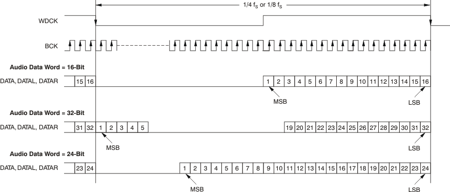 Figure 59. Audio Data Input Format for External Digital Filter (Internal DF Bypass Mode) Application
8.2.2.2.4 System Clock (SCK) and Interface Timing
The PCM1795 device in an application using an external digital filter requires the synchronization of WDCK and the system clock. The system clock is phase-free with respect to WDCK. Interface timing among WDCK, BCK, DATA, DATAL, and DATAR is shown in Figure 60 and Table 32.
 Figure 60. Audio Interface Timing for External Digital Filter (Internal DF Bypass Mode) Application
Table 32. Timing Characteristics for Figure 60
| MIN | MAX | UNIT | ||
|---|---|---|---|---|
| t(BCY) | BCK pulse cycle time | 20 | ns | |
| t(BCL) | BCK pulse duration, low | 7 | ns | |
| t(BCH) | BCK pulse duration, high | 7 | ns | |
| t(BL) | BCK rising edge to WDCK falling edge | 5 | ns | |
| t(LB) | WDCK falling edge to BCK rising edge | 5 | ns | |
| t(DS) | DATA, DATAL, DATAR setup time | 5 | ns | |
| t(DH) | DATA, DATAL, DATAR hold time | 5 | ns | |
8.2.2.2.5 Functions Available in the External Digital Filter Mode
The external digital filter mode is selected by setting DSD = 0 (register 20, B5) and DFTH = 1 (register 20, B4).
The external digital filter mode allows access to the majority of the PCM1795 mode control functions.
Table 33 shows the register mapping available when the external digital filter mode is selected, along with descriptions of functions that are modified when using this mode selection.
Table 33. External Digital Filter Register Map
| REGISTER | B15 | B14 | B13 | B12 | B11 | B10 | B9 | B8 | B7 | B6 | B5 | B4 | B3 | B2 | B1 | B0 |
|---|---|---|---|---|---|---|---|---|---|---|---|---|---|---|---|---|
| Register 16 | R/W | 0 | 0 | 1 | 0 | 0 | 0 | 0 | X(1) | X | X | X | X | X | X | X |
| Register 17 | R/W | 0 | 0 | 1 | 0 | 0 | 0 | 1 | X | X | X | X | X | X | X | X |
| Register 18 | R/W | 0 | 0 | 1 | 0 | 0 | 1 | 0 | X | FMT2 | FMT1 | FMT0 | X | X | X | X |
| Register 19 | R/W | 0 | 0 | 1 | 0 | 0 | 1 | 1 | REV | X | X | OPE | X | DFMS | X | INZD |
| Register 20 | R/W | 0 | 0 | 1 | 0 | 1 | 0 | 0 | X | SRST | 0 | 1 | MONO | CHSL | OS1 | OS0 |
| Register 21 | R/W | 0 | 0 | 1 | 0 | 1 | 0 | 1 | X | X | X | X | X | X | X | PCMZ |
| Register 22 | R | 0 | 0 | 1 | 0 | 1 | 1 | 0 | X | X | X | X | X | X | ZFGR | ZFGL |
8.2.2.2.5.1 FMT[2:0]: Audio Data Format Selection
Default value: 000
Table 34. FMT[2:0]
| FMT[2:0] | AUDIO DATA FORMAT SELECTION |
|---|---|
| 000 | 16-bit right-justified format |
| 001 | 32-bit right-justified format |
| 010 | 24-bit right-justified format (default) |
| Other | N/A |
8.2.2.2.5.2 OS[1:0]: ΔΣ Modulator Oversampling Rate Selection
Default value: 00
Table 35. OS[1:0]
| OS[1:0] | OPERATION SPEED SELECTION |
|---|---|
| 00 | 8 times WDCK (default) |
| 01 | 4 times WDCK |
| 10 | 16 times WDCK |
| 11 | Reserved |
The effective oversampling rate is determined by the oversampling performed by both the external digital filter and the ΔΣ modulator. For example, if the external digital filter is 8× oversampling, and OS[1:0] = 00 is selected, then the ΔΣ modulator oversamples by 8×, resulting in an effective oversampling rate of 64×. The 16× WDCK oversampling rate is not available above a 100-kHz sampling rate. If the oversampling rate selected is 16× WDCK, the system clock frequency must be over 256 fS.
8.2.2.3 Application Curves
 Figure 61. Amplitude vs Frequency
 Figure 62. Amplitude vs Frequency
8.2.3 Application for DSD Format (DSD Mode) Interface
Figure 63 shows a connection diagram for DSD mode.
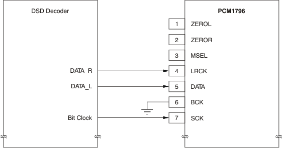 Figure 63. Connection Diagram in DSD Mode
8.2.3.1 Design Requirements
- Control: Host controller with SPI communication
- Audio Output: I/V output circuitry
- Audio Input: DSD Digital Audio input
8.2.3.2 Detailed Design Procedure
8.2.3.2.1 Features
This mode is used for interfacing directly to a DSD decoder, which is found in Super Audio CD™ (SACD) applications.
The DSD mode is accessed by programming the following bit in the corresponding control register.
- DSD = 1 (register 20)
The DSD mode provides a low-pass filtering function. The filtering is provided using an analog FIR filter structure. Four FIR responses are available and are selected by the DMF[1:0] bits of control register 18.
The DSD bit must be set before inputting DSD data; otherwise, the PCM1795 erroneously detects the TDMCA mode and commands are not accepted through the serial control interface.
8.2.3.2.2 Pin Assignment When Using DSD Format Interface
Several pins are redefined for DSD mode operation. These include:
- DATA (pin 5): DSDL as left-channel DSD data input
- LRCK (pin 4): DSDR as right-channel DSD data input
- SCK (pin 7): DBCK as bit clock for DSD data
- BCK (pin 6): Set low (N/A)
8.2.3.2.3 Requirements for System Clock
For operation in DSD mode, the bit clock (DBCK) is required on pin 7 of the PCM1795. The frequency of the bit clock can be N times the sampling frequency. Generally, N is 64 in DSD applications.
The interface timing between the bit clock and DSDL and DSDR is required to meet the setup and hold time specifications shown in Figure 65 and Table 36.
 Figure 64. Normal Data Output Form From DSD Decoder
 Figure 65. Timing for DSD Audio Interface
Table 36. Timing Characteristics for Figure 65
| MIN | MAX | UNIT | ||
|---|---|---|---|---|
| t(BCY) | DBCK pulse cycle time | 85(1) | ns | |
| t(BCH) | DBCK high-level time | 30 | ns | |
| t(BCL) | DBCK low-level time | 30 | ns | |
| t(DS) | DSDL, DSDR setup time | 10 | ns | |
| t(DH) | DSDL, DSDR hold time | 10 | ns | |
8.2.3.2.4 DSD Mode Configuration and Function Controls
8.2.3.2.4.1 Configuration for the DSD Interface Mode
The DSD interface mode is selected by setting DSD = 1 (register 20, B5).
Table 37. DSD Mode Register Map
| REGISTER | B15 | B14 | B13 | B12 | B11 | B10 | B9 | B8 | B7 | B6 | B5 | B4 | B3 | B2 | B1 | B0 |
|---|---|---|---|---|---|---|---|---|---|---|---|---|---|---|---|---|
| Register 16 | R/W | 0 | 0 | 1 | 0 | 0 | 0 | 0 | X(1) | X | X | X | X | X | X | X |
| Register 17 | R/W | 0 | 0 | 1 | 0 | 0 | 0 | 1 | X | X | X | X | X | X | X | X |
| Register 18 | R/W | 0 | 0 | 1 | 0 | 0 | 1 | 0 | X | X | X | X | DMF1 | DMF0 | X | X |
| Register 19 | R/W | 0 | 0 | 1 | 0 | 0 | 1 | 1 | REV | X | X | OPE | X | X | X | X |
| Register 20 | R/W | 0 | 0 | 1 | 0 | 1 | 0 | 0 | X | SRST | 1 | X | MONO | CHSL | OS1 | OS0 |
| Register 21 | R | 0 | 0 | 1 | 0 | 1 | 0 | 1 | X | X | X | X | X | DZ1 | DZ0 | X |
| Register 22 | R | 0 | 0 | 1 | 0 | 1 | 1 | 0 | X | X | X | X | X | X | ZFGR | ZFGL |
8.2.3.2.4.2 DMF[1:0]: Analog-FIR Performance Selection
Default value: 00
Table 38. DMF[1:0]
| DMF[1:0] | ANALOG-FIR PERFORMANCE SELECTION |
|---|---|
| 00 | FIR-1 (default) |
| 01 | FIR-2 |
| 10 | FIR-3 |
| 11 | FIR-4 |
Plots for the four analog finite impulse response (FIR) filter responses are shown in Analog FIR Filter Performance in DSD Mode.
8.2.3.2.4.3 OS[1:0]: Analog-FIR Operation-Speed Selection
Default value: 00
Table 39. OS[1:0]
| OS[1:0] | OPERATING SPEED SELECTION |
|---|---|
| 00 | fDBCK (default) |
| 01 | fDBCK/2 |
| 10 | Reserved |
| 11 | fDBCK/4 |
The OS bit in the DSD mode is used to select the operating rate of the analog FIR. The OS bits must be set before setting the DSD bit to '1'.
8.2.3.3 Application Curves
 Figure 66. Amplitude vs Frequency
 Figure 67. Amplitude vs Frequency
8.2.4 TDMCA Interface Format
The PCM1795 device supports the time-division-multiplexed command and audio (TDMCA) data format to simplify the host control serial interface. TDMCA format is designed not only for the multichannel buffered serial port description (McBSP) of TI DSPs but also for any programmable devices. TDMCA format can transfer not only audio data but also command data, so that it can be used together with any kind of device that supports TDMCA format. The TDMCA frame consists of a command field, extended command field, and some audio data fields. Those audio data are transported to IN devices (such as a DAC) and/or from OUT devices (such as an ADC). The PCM1795 is an IN device. LRCK and BCK are used with both IN and OUT devices so that the sample frequency of all devices in a system must be the same. The TDMCA mode supports a maximum of 30 device IDs. The maximum number of audio channels depends on the BCK frequency.
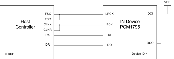 Figure 68. TDMCA Diagram
8.2.4.1 Design Requirements
- Control: TDMCA control information
- Audio Input: TDMCA input with LRCK signal with a pulse of two BCK clocks
- Audio Output: I/V output circuitry
8.2.4.2 Detailed Design Procedure
8.2.4.2.1 TDMCA Mode Determination
The PCM1795 device recognizes the TDMCA mode automatically when it receives an LRCK signal with a pulse duration of two BCK clocks. If the TDMCA mode operation is not needed, the duty cycle of LRCK must be 50%. Figure 69 shows the LRCK and BCK timing that determines the TDMCA mode. The PCM1795 device enters TDMCA mode after two continuous TDMCA frames. Any TDMCA commands can be issued during the next TDMCA frame after entering TDMCA mode.
 Figure 69. LRCK and BCK Timing for Determination of TDMCA Mode
8.2.4.2.2 TDMCA Terminals
TDMCA requires six signals: four signals are for the command and audio data interface, and one pair for daisy-chaining. These signals can be shared as shown in Table 40. The DO signal has a 3-state output so that it can be connected directly to other devices.
Table 40. TDMCA Terminals
| TERMINAL NAME | TDMCA NAME | PROPERTY | DESCRIPTION |
|---|---|---|---|
| LRCK | LRCK | Input | TDMCA frame start signal; it must be the same as the sampling frequency |
| BCK | BCK | Input | TDMCA clock; its frequency must be high enough to communicate a TDMCA frame within an LRCK cycle |
| DATA | DI | Input | TDMCA command and audio data input signal |
| MDO | DO | Output | TDMCA command data 3-state output signal |
| MC | DCI | Input | TDMCA daisy-chain input signal |
| MS | DCO | Output | TDMCA daisy-chain output signal |
8.2.4.2.3 Device ID Determination
TDMCA mode also supports a multichip implementation in one system. This capability means that a host controller (DSP) can simultaneously support several TDMCA devices, which can be of the same type or different types, including PCM devices. The PCM devices are categorized as either IN devices, OUT devices, IN/OUT devices, and NO devices. The IN device has an input port to receive audio data; the OUT device has an output port to supply audio data; the IN/OUT device has both input and output ports for audio data; and the NO device has no port for audio data, but requires command data from the host. A DAC is an IN device; an ADC is an OUT device; a codec is an IN/OUT device; and a PLL is a NO device. The PCM1795 is an IN device. For the host controller to distinguish the devices, each device is assigned its own device ID by the daisy-chain. The devices obtain their own device IDs automatically by connecting the DCI to the DCO of the preceding device and the DCO to the DCI of the following device in the daisy-chain. The daisy-chains are categorized as the IN chain and the OUT chain, which are completely independent and equivalent. Figure 70 shows an example daisy-chain connection. If a system must chain the PCM1795 device and a NO device in the same IN or OUT chain, the NO device must be chained at the back end of the chain because it does not require any audio data. Figure 71 shows an example TDMCA system including an IN chain and an OUT chain with a TI DSP. For a device to get its own device ID, the DID signal must be set to '1' (see the Command Field section for details), and LRCK and BCK must be driven in the TDMCA mode for all PCM devices that are chained. The device at the top of the chain knows its device ID is '1' because its DCI is fixed high. Other devices count the BCK pulses and observe the respective DCI signal to determine ID and position in the chain. Figure 72 shows the initialization of each device ID.
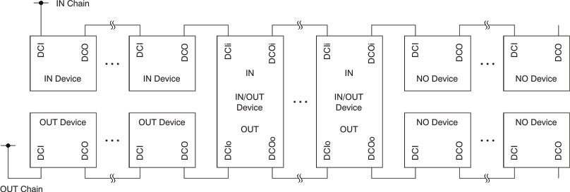 Figure 70. Daisy-Chain Connection Example
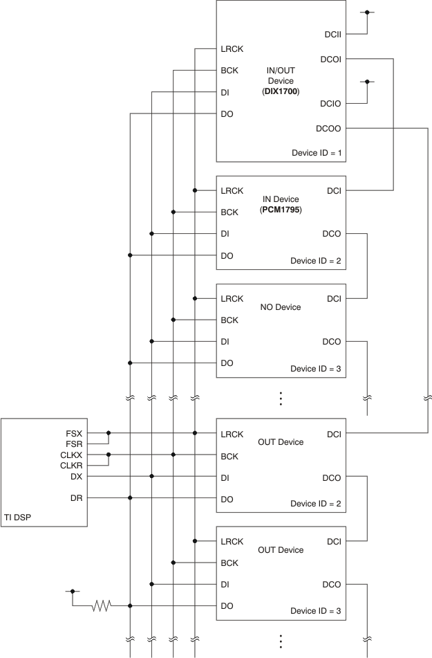 Figure 71. IN Daisy-Chain and OUT Daisy-Chain Connection Example for a Multichip System
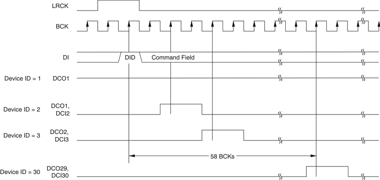 Figure 72. Device ID Determination Sequence
8.2.4.2.4 TDMCA Frame
In general, the TDMCA frame consists of the command field, extended command (EMD) field, and audio data fields. All fields are 32 bits long, but the lowest byte has no meaning. The MSB is transferred first for each field. The command field is always transferred as the first packet of the frame. The EMD field is transferred if the EMD flag of the command field is high. If any EMD packets are transferred, no audio data follow the EMD packets. This frame is for quick system initialization. All devices of a daisy-chain should respond to the command field and extended command field. The PCM1795 has two audio channels that can be selected by OPE (register 19). If the OPE bit is not set to high, those audio channels are transferred. Figure 73 shows the general TDMCA frame. If some DACs are enabled, but corresponding audio data packets are not transferred, the analog outputs are unpredictable.
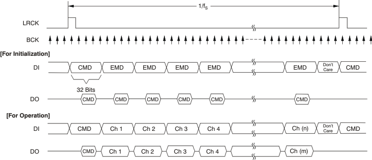 Figure 73. General TDMCA Frame
 Figure 74. TDMCA Frame Example of Six-Channel DAC and Two-Channel ADC With Command Read
8.2.4.2.5 Command Field
The normal command field is defined as shown in Figure 75. When the DID bit (MSB) is '1', this frame is used only for device ID determination, and all remaining bits in the field are ignored.
 Figure 75. Normal Command Field
8.2.4.2.5.1 Bit 31: Device ID Enable Flag
The PCM1795 operates to get its own device ID for TDMCA initialization if this bit is high.
8.2.4.2.5.2 Bit 30: Extended Command Enable Flag
The EMD packet is transferred if this bit is high; otherwise, it is skipped. Once this bit is high, this frame does not contain any audio data. This is for system initialization.
8.2.4.2.5.3 Bit 29: Daisy-Chain Selection Flag
A high setting designates OUT-chain devices, low designates IN-chain devices. The PCM1795 is an IN device, so the DCS bit must be set low.
8.2.4.2.5.4 Bits[28:24]: Device ID
The device ID is 5 bits long and it can be defined. These bits identify the order of a device in the IN or OUT daisy-chain. The top of the daisy-chain defines device ID 1 and successive devices are numbered 2, 3, 4, etc. All devices for which the DCI is fixed high are also defined as ID 1. The maximum device ID is 30 each in the IN and OUT chains. If a device ID of 0x1F is used, all devices are selected as broadcast when in the write mode. If a device ID of 0x00 is used, no device is selected.
8.2.4.2.5.5 Bit 23: Command Read/Write flag
If this bit is high, the command is a read operation.
8.2.4.2.5.6 Bits[22:16]: Register ID
The register ID is 7 bits long.
8.2.4.2.5.7 Bits[15:8]: Command data
The command data are 8 bits long. Any valid data can be chosen for each register.
8.2.4.2.5.8 Bits[7:0]: Not used
These bits are never transported when a read operation is performed.
8.2.4.2.6 Extended Command Field
The extended command field is the same as the command field, except that it does not have a DID flag. Figure 76 defines the extended command field.
 Figure 76. Extended Command Field
8.2.4.2.7 Audio Fields
The audio field is 32 bits long and the audio data are transferred MSB first, so the other fields must be filled with 0s as shown in Figure 77.
 Figure 77. Audio Field Example
8.2.4.2.8 TDMCA Register Requirements
The TDMCA mode requires device ID and audio channel information, as previously described. The OPE bit in register 19 indicates audio channel availability and register 23 indicates the device ID. Register 23 is used only in the TDMCA mode; see the mode control register map of Table 10.
8.2.4.2.9 Register Write/Read Operation
The command supports register write and read operations. If the command requests to read one register, the read data are transferred on DO during the data phase of the timing cycle. The DI signal can be retrieved at the positive edge of BCK, and the DO signal is driven at the negative edge of BCK. DO is activated one BCK cycle early to compensate for the output delay caused by high impedance. Figure 78 shows the TDMCA write and read timing.
 Figure 78. TDMCA Write and Read Operation Timing
8.2.4.2.10 TDMCA Mode Operation
DCO specifies the owner of the next audio channel in TDMCA mode operation. When a device retrieves its own audio channel data, DCO goes high during the last audio channel period. Figure 79 shows the DCO output timing in TDMCA mode operation. The host controller ignores the behavior of DCI and DCO. DCO indicates the last audio channel of each device. Therefore, DCI means the next audio channel is allocated.
If some devices are skipped because of no active audio channel, the skipped devices must notify the next device that the DCO will be passed through the next DCI. Figure 80 and Figure 81 show DCO timing with skip operation. Figure 82 and Table 41 show the ac timing of the daisy-chain signals.
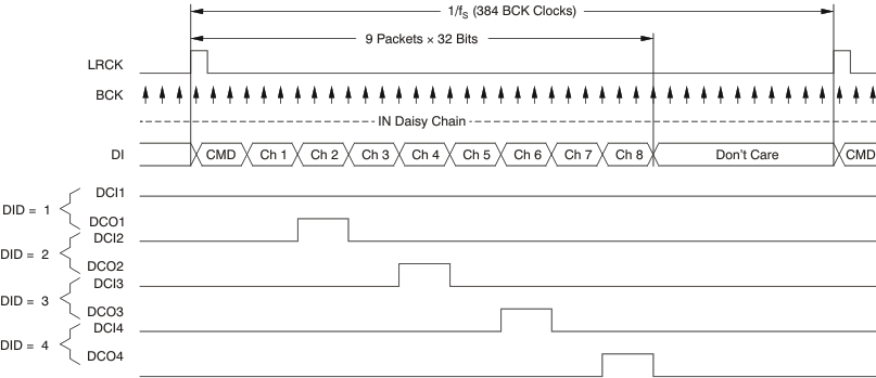 Figure 79. DCO Output Timing of TDMCA Mode Operation
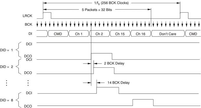 Figure 80. DCO Output Timing With Skip Operation
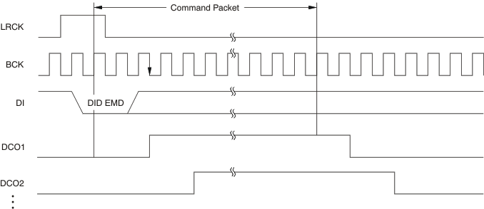 Figure 81. DCO Output Timing With Skip Operation (for Command Packet 1)
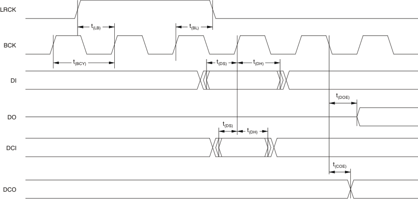 Figure 82. AC Timing of Daisy-Chain Signals
Table 41. Timing Characteristics for Figure 82
| MIN | MAX | UNIT | ||
|---|---|---|---|---|
| t(BCY) | BCK pulse cycle time | 20 | ns | |
| t(LB) | LRCK setup time | 0 | ns | |
| t(BL) | LRCK hold time | 3 | ns | |
| t(DS) | DI setup time | 0 | ns | |
| t(DH) | DI hold time | 3 | ns | |
| t(DS) | DCI setup time | 0 | ns | |
| t(DH) | DCI hold time | 3 | ns | |
| t(DOE) | DO output delay(1) | 8 | ns | |
| t(COE) | DCO output delay(1) | 6 | ns | |
