ZHCSCT4A September 2014 – January 2017 REF1925 , REF1930 , REF1933 , REF1941
PRODUCTION DATA.
9 Detailed Description
9.1 Overview
The REF19xx is a family of dual-output, VREF and VBIAS (VREF / 2) band-gap voltage references. The Functional Block Diagram section provides a block diagram of the basic band-gap topology and the two buffers used to derive the VREF and VBIAS outputs. Transistors Q1 and Q2 are biased such that the current density of Q1 is greater than that of Q2. The difference of the two base emitter voltages (VBE1 – VBE2) has a positive temperature coefficient and is forced across resistor R5. The voltage is amplified and added to the base emitter voltage of Q2, which has a negative temperature coefficient. The resulting band-gap output voltage is almost independent of temperature. Two independent buffers are used to generate VREF and VBIAS from the band-gap voltage. The resistors R1, R2 and R3, R4 are sized such that VBIAS = VREF / 2.
e-Trim™ is a method of package-level trim for the initial accuracy and temperature coefficient of VREF and VBIAS, implemented during the final steps of manufacturing after the plastic molding process. This method minimizes the influence of inherent transistor mismatch, as well as errors induced during package molding. e-Trim is implemented in the REF19xx to minimize the temperature drift and maximize the initial accuracy of both the VREF and VBIAS outputs.
9.2 Functional Block Diagram

9.3 Feature Description
9.3.1 VREF and VBIAS Tracking
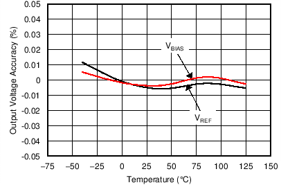
Most single-supply systems require an additional stable voltage in the middle of the analog-to-digital converter (ADC) input range to bias input bipolar signals. The VREF and VBIAS outputs of the REF19xx are generated from the same band-gap voltage as shown in the Functional Block Diagram section. Hence, both outputs track each other over the full temperature range of –40°C to 125°C with an accuracy of 7 ppm/°C (max). The tracking accuracy increases to 6 ppm/°C (max) when the temperature range is limited to –40°C to 85°C. The tracking error is calculated using the box method, as described by Equation 2:
where
The tracking accuracy is as shown in Figure 44.
 Figure 44. VREF and VBIAS Tracking vs Temperature
9.3.2 Low Temperature Drift
The REF19xx is designed for minimal drift error, which is defined as the change in output voltage over temperature. The drift is calculated using the box method, as described by Equation 3:

9.3.3 Load Current
The REF19xx family is specified to deliver a current load of ±20 mA per output. Both the VREF and VBIAS outputs of the device are protected from short circuits by limiting the output short-circuit current to 50 mA. The device temperature increases according to Equation 4:

where
- TJ = junction temperature (°C),
- TA = ambient temperature (°C),
- PD = power dissipated (W), and
- RθJA = junction-to-ambient thermal resistance (°C/W).
The REF19xx maximum junction temperature must not exceed the absolute maximum rating of 150°C.
9.4 Device Functional Modes
When the EN pin of the REF19xx is pulled high, the device is in active mode. The device must be in active mode for normal operation. The REF19xx can be placed in a low-power mode by pulling the ENABLE pin low. When in shutdown mode, the output of the device becomes high impedance and the quiescent current of the device reduces to 5 µA in shutdown mode. See the Electrical Characteristics for logic high and logic low voltage levels.
