ZHCSDS0B July 2011 – May 2015 SM74101
PRODUCTION DATA.
8 Application and Implementation
NOTE
Information in the following applications sections is not part of the TI component specification, and TI does not warrant its accuracy or completeness. TI’s customers are responsible for determining suitability of components for their purposes. Customers should validate and test their design implementation to confirm system functionality.
8.1 Application Information
The SM74101 can be used to drive a low side MOSFET with very low switching losses. Either one of the control input pins, IN or INB, can be used to control the gate drive to the MOSFET. The choice of the control input pin used will depend on the polarity of operation.
8.2 Typical Application
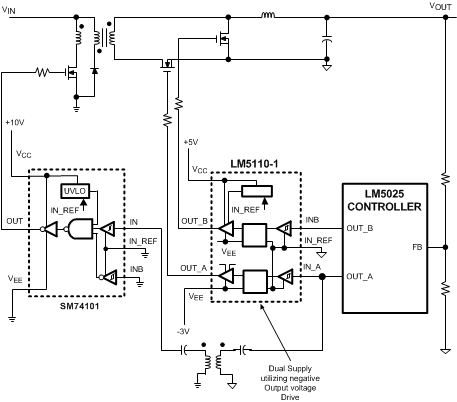
The SM74101 is utilized in a DC/DC forward topology power supply as shown in Figure 14. The high peak gate drive current of the SM74101 allows for short rise and fall times on the primary side MOSFET, thereby improving overall efficiency of the system and reducing switching losses. It is used in conjunction with the LM5025 Active Clamp Voltage Mode PWM Controller to provide drive capability to the primary side MOSFET after isolation.
 Figure 14. DC/DC Forward Topology Power Supply
8.2.1 Design Requirements
The SM74101 is used in the non-inverting mode of operation. The IN pin is used to control the OUT signal to the primary side MOSFET. The signal that travels from OUT_A and through the isolation transformer should be compatible with the high and low threshold voltages of the IN pin. INB is not used in this mode and is therefore connected to IN_REF, which is also the primary side ground.
8.2.2 Detailed Design Procedure
See Power Supply Recommendations, Layout, and Thermal Considerations for key design considerations regarding the input supply, grounding, and thermal calculations specific to the SM74101.
8.2.3 Application Curve
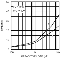
The rise and fall times of the OUT signal will depend on the capacitance of the MOSFET gate. Therefore, an appropriate MOSFET should be selected to meet the switching speed and efficiency requirements of the system.
 Figure 15. Rise and Fall Time vs Capacitive Load