SDLS144D April 1985 – October 2016 SN54LS240 , SN54LS241 , SN54LS244 , SN54S240 , SN54S241 , SN54S244 , SN74LS240 , SN74LS241 , SN74LS244 , SN74S240 , SN74S241 , SN74S244
- 1 Features
- 2 Applications
- 3 Description
- 4 Revision History
- 5 Pin Configuration and Functions
-
6 Specifications
- 6.1 Absolute Maximum Ratings
- 6.2 ESD Ratings
- 6.3 Recommended Operating Conditions
- 6.4 Thermal Information
- 6.5 Electrical Characteristics - SNx4LS24x
- 6.6 Electrical Characteristics - SNx4S24x
- 6.7 Switching Characteristics - SNx4LS24x
- 6.8 Switching Characteristics - SNx4S24x
- 6.9 Typical Characteristics
- 7 Parameter Measurement Information
- 8 Detailed Description
- 9 Application and Implementation
- 10Power Supply Recommendations
- 11Layout
- 12Device and Documentation Support
- 13Mechanical, Packaging, and Orderable Information
封装选项
机械数据 (封装 | 引脚)
散热焊盘机械数据 (封装 | 引脚)
订购信息
8 Detailed Description
8.1 Overview
This device is organized as two 4-bit buffers and drivers with separate output-enable (G) inputs. When G is low, the device passes data from the A inputs to the Y outputs. When G is high, the outputs are in the high impedance state. Inputs can be driven from either 3.3-V or 5-V devices. This feature allows the use of this device as a translator in a mixed 3.3-V and 5-V system environment. To ensure the high-impedance state during power up or power down, G must be tied to VCC through a pullup resistor; the minimum value of the resistor is determined by the current-sinking capability of the driver.
8.2 Functional Block Diagrams
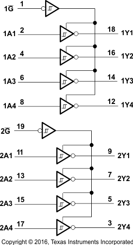
Logic Diagram
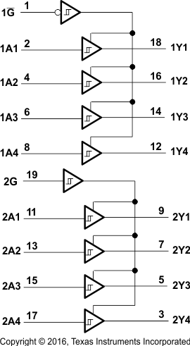
Logic Diagram
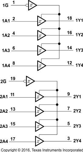
Logic Diagram
8.3 Feature Description
8.3.1 3-State Outputs
The 3-state outputs can drive bus lines directly. All outputs can be put into high impedance mode through the G pin.
8.3.2 PNP Inputs
This device has PNP inputs which reduce dc loading on bus lines.
8.3.3 Hysteresis on Bus Inputs
The bus inputs have built-in hysteresis that improves noise margins.
8.4 Device Functional Modes
The SNx4LS24x and SNx4S24x devices can be used as inverting and non-inverting bus buffers for data line transmission and can isolate input to output by setting the G pin HIGH. Table 1, Table 2, and Table 3 list the function tables for all devices.
Table 1. SNx4LS240 and SNx4S240
Function Table
| INPUTS | OUTPUTS | |
|---|---|---|
| G | A | Y |
| L | L | H |
| L | H | L |
| H | X | Z |
Table 2. SNx4LS241 and SNx4S241
Function Table
| CHANNEL 1 | CHANNEL 2 | ||||
|---|---|---|---|---|---|
| INPUTS | OUTPUT | INPUTS | OUTPUT | ||
| 1G | 1A | 1Y | 2G | 2A | 2Y |
| L | L | L | H | L | L |
| L | H | H | H | H | H |
| H | X | Z | L | X | Z |
Table 3. SNx4LS244 and SNx4S244
Function Table
| INPUTS | OUTPUTS | |
|---|---|---|
| G | A | Y |
| L | L | L |
| L | H | H |
| H | X | Z |
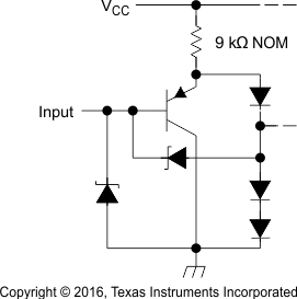 Figure 19. SNx4LS240, SNx4LS241, SNx4LS244
Equivalent of Each Input
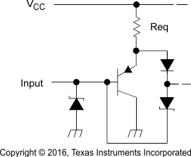
Equivalent of Each Input

R = 50 Ω NOM
R = 25 Ω NOM