ZHCSJ41 December 2018 SN55HVD233-SEP
PRODUCTION DATA.
- 1 特性
- 2 应用
- 3 说明
- 4 修订历史记录
- 5 说明 (续)
- 6 Pin Configuration and Functions
-
7 Specifications
- 7.1 Absolute Maximum Ratings
- 7.2 ESD Ratings
- 7.3 Recommended Operating Conditions
- 7.4 Thermal Information
- 7.5 Driver Electrical Characteristics
- 7.6 Receiver Electrical Characteristics
- 7.7 Driver Switching Characteristics
- 7.8 Receiver Switching Characteristics
- 7.9 Device Switching Characteristics
- 7.10 Typical Characteristics
- 8 Parameter Measurement Information
- 9 Detailed Description
- 10Application and Implementation
- 11Power Supply Recommendations
- 12Layout
- 13器件和文档支持
- 14机械、封装和可订购信息
10.1.1 Diagnostic Loopback
The diagnostic loopback or internal loopback function of the SN55HVD233-SEP is enabled with a high-level input on pin 7, LBK. This mode disables the driver output while keeping the bus pins biased to the recessive state. This mode also redirects the D data input (transmit data) through logic to the received data output (R), thus creating an internal loopback of the transmit-to-receive data path. This mimics the loopback that occurs normally with a CAN transceiver because the receiver loops back the driven output to the R (receive data) pin. This mode allows the host microprocessor to input and read back a bit sequence or CAN messages to perform diagnostic routines without disturbing the CAN bus. Figure 33 shows a typical CAN bus application.
If the LBK pin is not used, it may be tied to ground (GND). However, it is pulled low internally (defaults to a low-level input) and may be left open if not in use.
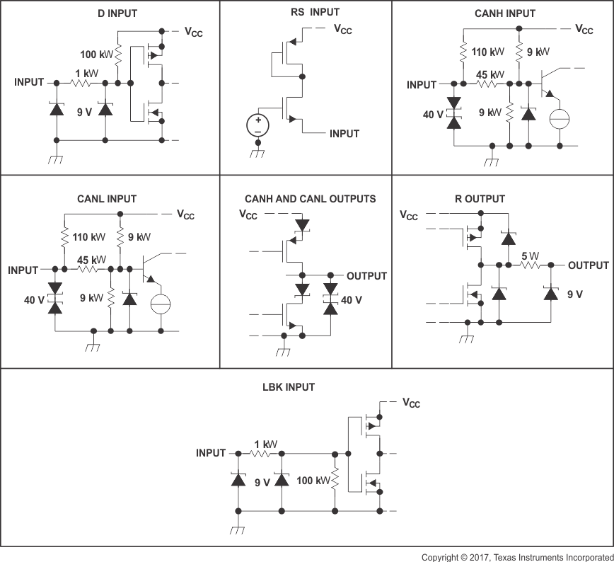
 Figure 28. Equivalent Input and Output Schematic Diagrams