SLLS516E August 2002 – July 2015 SN65LVDS100 , SN65LVDS101 , SN65LVDT100 , SN65LVDT101
UNLESS OTHERWISE NOTED, this document contains PRODUCTION DATA.
- 1 Features
- 2 Applications
- 3 Description
- 4 Revision History
- 5 Description (Continued)
- 6 Device Options
- 7 Pin Configuration and Functions
- 8 Specifications
- 9 Parameter Measurement Information
- 10Detailed Description
-
11Application and Implementation
- 11.1 Application Information
- 11.2
Typical Application
- 11.2.1 PECL to LVDS Translation
- 11.2.2 LVDS to 3.3-V PECL Translation
- 11.2.3 5-V PECL to 3.3-V PECL Translation
- 11.2.4 CML to LVDS or 3.3-V PECL Translation
- 11.2.5 Single-Ended 3.3-V PECL to LVDS Translation
- 11.2.6 Single-Ended CMOS to LVDS Translation
- 11.2.7 Single-Ended CMOS to 3.3-V PECL Translation
- 11.2.8 Receipt of AC-Coupled Signals
- 12Power Supply Recommendations
- 13Layout
- 14Device and Documentation Support
- 15Mechanical, Packaging, and Orderable Information
封装选项
请参考 PDF 数据表获取器件具体的封装图。
机械数据 (封装 | 引脚)
- D|8
- DGK|8
散热焊盘机械数据 (封装 | 引脚)
订购信息
8 Specifications
8.1 Absolute Maximum Ratings(1)
over operating free-air temperature range unless otherwise noted| MIN | MAX | UNIT | ||
|---|---|---|---|---|
| VCC | Supply voltage range(2) | –0.5 | 4 | V |
| IBB | VBB output current | –0.5 | 0.5 | mA |
| VI | Voltage range, (A, B, Y, Z) | 0 | 4.3 | V |
| VO | ||||
| VID | Differential voltage, |VA – VB| ('LVDT100 and 'LVDT101 only) | 1 | V |
(1) Stresses beyond those listed under Absolute Maximum Ratings may cause permanent damage to the device. These are stress ratings only, and functional operation of the device at these or any other conditions beyond those indicated under Recommended Operating Conditions is not implied. Exposure to absolute-maximum-rated conditions for extended periods may affect device reliability.
(2) All voltage values, except differential I/O bus voltages, are with respect to network ground terminal.
8.2 ESD Ratings
| VALUE | UNIT | ||||
|---|---|---|---|---|---|
| V(ESD) | Electrostatic discharge | Human body model (HBM), per ANSI/ESDA/JEDEC JS-001(1) | Pins 2, 3, 5, 6, 7 | ±5000 | V |
| All pins except 2, 3, 5, 6, 7 | ±2000 | V | |||
| Charged-device model (CDM), per JEDEC specification JESD22-C101(2) | ±1500 | V | |||
(1) Tested in accordance with JEDEC Standard 22, Test Method A114-A.7.
(2) Tested in accordance with JEDEC Standard 22, Test Method C101.
8.3 Recommended Operating Conditions
| MIN | NOM | MAX | UNIT | ||
|---|---|---|---|---|---|
| Supply voltage, VCC | 3 | 3.3 | 3.6 | V | |
| Magnitude of differential input voltage |VID| | 'LVDS100 or 'LVDS101 | 0.1 | 1 | V | |
| 'LVDT100 or 'LVDT101 | 0.1 | 0.8 | |||
| Input voltage (any combination of common-mode or input signals), VI | 0 | 4 | V | ||
| VBB output current, IO(VBB) | –400(1) | 12 | µA | ||
| Operating free-air temperature, TA | –40 | 85 | °C | ||
(1) The algebraic convention, in which the less positive (more negative) limit is designated minimum, is used in this data sheet.
8.4 Thermal Information
| THERMAL METRIC(1) | SN65LVDS100, SN65LVDT100, SN65LVDS101, SN65LVDT101 | UNIT | ||
|---|---|---|---|---|
| D | DGK | |||
| 8 PINS | 8 PINS | |||
| RθJA | Junction-to-ambient thermal resistance | 208 | 263 | °C/W |
| Power dissipation rating: TA ≤ 25°C | 151 | 377 | mW | |
| Power dissipation rating: TA ≤ 85°C | 192 | 481 | ||
(1) For more information about traditional and new thermal metrics, see the IC Package Thermal Metrics application report, SPRA953.
8.5 Electrical Characteristics
over recommended operating conditions (unless otherwise specified)| PARAMETER | TEST CONDITIONS | MIN | TYP(1) | MAX | UNIT | |
|---|---|---|---|---|---|---|
| ICC | Supply current, 'LVDx100 | No load or input | 25 | 30 | mA | |
| Supply current, 'LVDx101 | RL = 50 Ω to 1 V, No input | 50 | 61 | |||
| PD | Device power dissipation, 'LVDx100 | RL = 100 Ω, No input | 110 | mW | ||
| Device power dissipation, 'LVDx101 | Y and Z to VCC – 2 V through 50 Ω No input |
116 | 142 | |||
| VBB | Reference voltage output, 'LVDS100 or 'LVDS101 | IO = –400 µA or 12 µA | VCC – 1.4 | VCC – 1.35 | VCC – 1.3 | mV |
| SN65LVDS100 and SN65LVDS101 INPUT CHARACTERISTICS (see Figure 30) | ||||||
| VIT+ | Positive-going differential input voltage threshold | See Figure 30 and Table 1 | 100 | mV | ||
| VIT– | Negative-going differential input voltage threshold | –100 | ||||
| II | Input current | VI = 0 V or 2.4 V Second input at 1.2 V |
–20 | 20 | µA | |
| VI = 4 V, Second input at 1.2 V | 33 | µA | ||||
| II(OFF) | Power off input current | VCC = 1.5 V, VI = 0 V or 2.4 V Second input at 1.2 V |
–20 | 20 | µA | |
| VCC = 1.5 V, VI = 4 V Second input at 1.2 V |
33 | |||||
| IIO | Input offset current (|IIA - IIB|) | VIA = VIB, 0 ≤ VIA ≤ 4 V | –6 | 6 | µA | |
| Ci | Small-signal input capacitance to GND | VI = 1.2 V | 0.6 | pF | ||
| SN65LVDT100 and SN65LVDT101 INPUT CHARACTERISTICS (see Figure 30) | ||||||
| VIT+ | Positive-going differential input voltage threshold | See Figure 30 and Table 1 | 100 | mV | ||
| VIT– | Negative-going differential input voltage threshold | –100 | ||||
| II | Input current | VI = 0 V or 2.4 V, Other input open | –40 | 40 | µA | |
| VI = 4 V, Other input open | 66 | |||||
| II(OFF) | Power off input current | VCC = 1.5 V, VI = 0 V or 2.4 V Other input open |
–40 | 40 | µA | |
| VCC = 1.5 V, VI = 4 V Other input open |
66 | |||||
| R(T) | Differential input resistance | VID = 300 mV or 500 mV VIC = 0 V or 2.4 V |
90 | 110 | 132 | Ω |
| VCC = 0 V, VID = 300 mV or 500 mV VIC = 0 V or 2.4 V |
90 | 110 | 132 | |||
| Ci | Small-signal differential input capacitance | VI = 1.2 V | 0.6 | pF | ||
| SN65LVDS100 and SN65LVDT100 OUTPUT CHARACTERISTICS (see Figure 30) | ||||||
| |VOD| | Differential output voltage magnitude | See Figure 31 | 247 | 340 | 454 | mV |
| Δ|VOD| | Change in differential output voltage magnitude between logic states | –50 | 50 | |||
| VOC(SS) | Steady-state common-mode output voltage | See Figure 32 | 1.125 | 1.375 | V | |
| ΔVOC(SS) | Change in steady-state common-mode output voltage between logic states | –50 | 50 | mV | ||
| VOC(PP) | Peak-to-peak common-mode output voltage | 50 | 150 | mV | ||
| IOS | Short-circuit output current | VO(Y) or VO(Z) = 0 V | –24 | 24 | mA | |
| IOS(D) | Differential short-circuit output current | VOD = 0 V | –12 | 12 | mA | |
| SN65LVDS101 and SN65LVDT101 OUTPUT CHARACTERISTICS (see Figure 30) | ||||||
| VOH | High-level output voltage | 50 Ω to VCC – 2 V, See Figure 39 | VCC – 1.25 | VCC – 1.02 | VCC – 0.9 | V |
| VCC = 3.3 V, 50-Ω load to 2.3 V | 2055 | 2280 | 2405 | mV | ||
| VOL | Low-level output voltage | 50 Ω to VCC – 2 V, See Figure 39 | VCC – 1.83 | VCC – 1.61 | VCC – 1.53 | V |
| VCC = 3.3 V, 50-Ω load to 2.3 V | 1475 | 1690 | 1775 | mV | ||
| |VOD| | Differential output voltage magnitude | 50-Ω load to VCC – 2 V, See Figure 39 | 475 | 575 | 750 | mV |
(1) Typical values are with a 3.3-V supply voltage and room temperature
8.6 Switching Characteristics
over recommended operating conditions (unless otherwise noted)| PARAMETER | TEST CONDITIONS | MIN | TYP(1) | MAX | UNIT | ||
|---|---|---|---|---|---|---|---|
| tPLH | Propagation delay time, low-to-high-level output | 'LVDx100 | See Figure 33 | 300 | 470 | 800 | ps |
| 'LVDx101 | 400 | 630 | 900 | ||||
| tPHL | Propagation delay time, high-to-low-level output | 'LVDx100 | 300 | 470 | 800 | ps | |
| 'LVDx100 | 400 | 630 | 900 | ||||
| tr | Differential output signal rise time (20% to 80%) | 220 | ps | ||||
| tf | Differential output signal fall time (20% to 80%) | 220 | ps | ||||
| tsk(p) | Pulse skew (|tPHL – tPLH|)(2) | 5 | 50 | ps | |||
| tsk(pp) | Part-to-part skew(3) | VID = 0.2 V, See Figure 33 | 100 | ps | |||
| tjit(per) | RMS period jitter(4) | 1 GHz 50% duty-cycle square-wave input VID = 200 mV, VIC = 1.2 V See Figure 34 |
1 | 3.7 | ps | ||
| tjit(cc) | Peak cycle-to-cycle jitter(5) | 6 | 23 | ps | |||
| tjit(pp) | Peak-to-peak jitter | 2 GHz PRBS, 223 – 1 run length VID = 200 mV, VIC = 1.2 V See Figure 34 |
28 | 65 | ps | ||
| tjit(det) | Peak-to-peak deterministic jitter(6) | 2 GHz PRBS, 27 – 1 run length VID = 200 mV, VIC = 1.2 V See Figure 34 |
17 | 48 | ps | ||
(1) All typical values are at 25°C and with a 3.3-V supply.
(2) tsk(p) is the magnitude of the time difference between the tPLH and tPHL of any output of a single device.
(3) tsk(pp) is the magnitude of the time difference in propagation delay time between any specified terminals of two devices when both devices operate with the same supply voltages, at the same temperature, and have identical packages and test circuits.
(4) Period jitter is the deviation in cycle time of a signal with respect to the ideal period over a random sample of 1,000,000 cycles.
(5) Cycle-to-cycle jitter is the variation in cycle time of a signal between adjacent cycles, over a random sample of 1,000 adjacent cycle pairs.
(6) Deterministic jitter is the sum of pattern-dependent jitter and pulse-width distortion.
8.7 Typical Characteristics
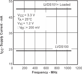 Figure 1. Supply Current vs Frequency
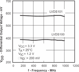 Figure 3. Differential Output Voltage vs Frequency
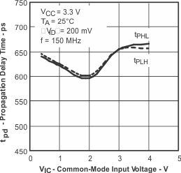 Figure 5. SN65LVDS101 Propagation Delay Time vs Common-Mode Input Voltage
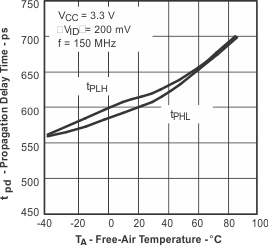 Figure 7. SN65LVDS101 Propagation Delay Time vs Free-Air Temperature
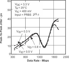 Figure 9. SN65LVDS100 Peak-to-Peak Jitter vs Data Rate
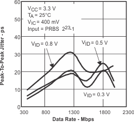 Figure 11. SN65LVDS101 Peak-to-Peak Jitter vs Data Rate
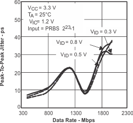 Figure 13. SN65LVDS100 Peak-to-Peak Jitter vs Data Rate
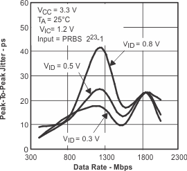 Figure 15. SN65LVDS101 Peak-to-Peak Jitter vs Data Rate
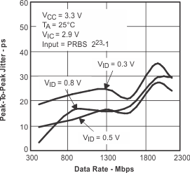 Figure 17. SN65LVDS100 Peak-to-Peak Jitter vs Data Rate
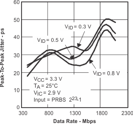 Figure 19. SN65LVDS101 Peak-to-Peak Jitter vs Data Rate
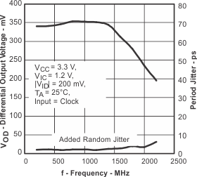 Figure 21. SN65LVDS100 Differential Output Voltage vs Frequency
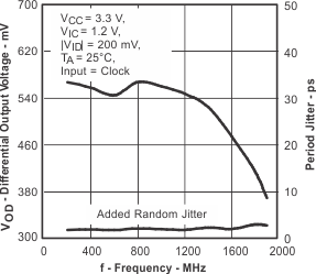 Figure 23. SN65LVDS101 Differential Output Voltage vs Frequency
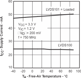 Figure 2. Supply Current vs Free-Air Temperature
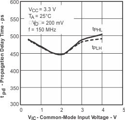 Figure 4. SN65LVDS100 Propagation Delay Time vs Common-Mode Input Voltage
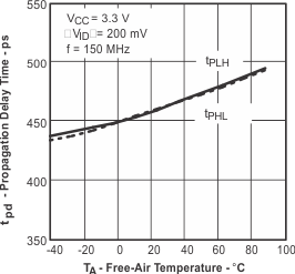 Figure 6. SN65LVDS100 Propagation Delay Time vs Free-Air Temperature
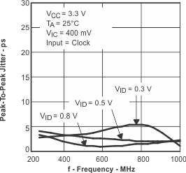 Figure 8. SN65LVDS100 Peak-to-Peak Jitter vs Frequency
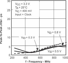 Figure 10. SN65LVDS101 Peak-to-Peak Jitter vs Frequency
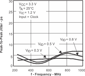 Figure 12. SN65LVDS100 Peak-to-Peak Jitter vs Frequency
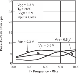 Figure 14. SN65LVDS101 Peak-to-Peak Jitter vs Frequency
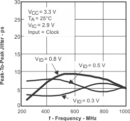 Figure 16. SN65LVDS100 Peak-to-Peak Jitter vs Frequency
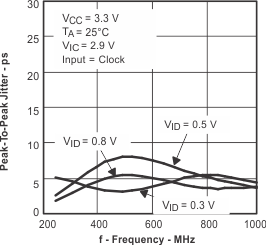 Figure 18. SN65LVDS101 Peak-to-Peak Jitter vs Frequency
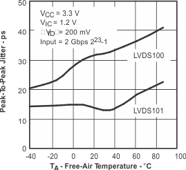 Figure 20. SN65LVDS100 Peak-to-Peak Jitter vs Free-Air Temperature
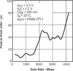 Figure 22. SN65LVDS100 Peak-to-Peak Jitter vs Data Rate
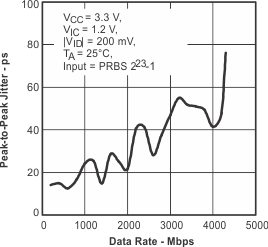 Figure 24. SN65LVDS101 Peak-to-Peak Jitter vs Data Rate
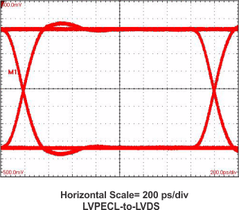 Figure 25. SN65LVDS100 Mbps, 223 – 1 PRBS
 Figure 27. SN65LVDS101 Mbps, 223 – 1 PRBS
NOTE:
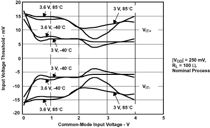
VIT is a steady-state parameter. The switching time is influenced by the input overdrive above this steady-state threshold up to a differential input voltage magnitude of 100 mV.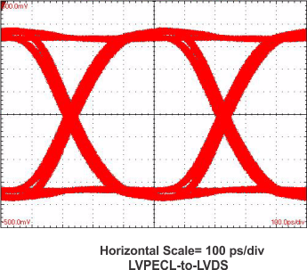 Figure 26. SN65LVDS100 Gbps, 223 – 1 PRBS
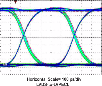 Figure 28. SN65LVDS101 Gbps, 223 – 1 PRBS