SCES656E February 2006 – November 2016 SN74LV4046A
PRODUCTION DATA.
- 1 Features
- 2 Applications
- 3 Description
- 4 Revision History
- 5 Pin Configuration and Functions
- 6 Specifications
- 7 Detailed Description
- 8 Application and Implementation
- 9 Power Supply Recommendations
- 10Layout
- 11Device and Documentation Support
- 12Mechanical, Packaging, and Orderable Information
封装选项
机械数据 (封装 | 引脚)
散热焊盘机械数据 (封装 | 引脚)
订购信息
8 Application and Implementation
NOTE
Information in the following applications sections is not part of the TI component specification, and TI does not warrant its accuracy or completeness. TI’s customers are responsible for determining suitability of components for their purposes. Customers should validate and test their design implementation to confirm system functionality.
8.1 Application Information
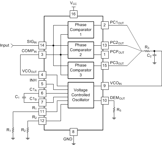
The most common use for the digital phased-locked loop (PLL) device is to match the VCO output to the same phase as the incoming signal and produce an error signal (DEMOUT) that indicates the amount of phase shift required for the match. This can be used as part of many complex systems.
8.2 Typical Application
 Figure 9. SN74LV4046A Digital Clock Signal Phase Comparison Application
8.2.1 Design Requirements
Table 1 and Table 2 lists the design requirements of the SN74LV4046A.
Table 1. Component Selection Criteria(1)
| COMPONENT | VALUE |
|---|---|
| R1 | 3 kΩ to 50 kΩ |
| R2 | 3 kΩ to 50 kΩ |
| R1 || R2 | > 2.7 kΩ |
| C1 | > 40 pF |
| R3 | 1 kΩ |
| C2 | 1 uF |
| R5 | 50 kΩ to 300 kΩ |
Table 2. CPD(1)
| CHIP SECTION | CPD | UNIT |
|---|---|---|
| Comparator 1 | 120 | pF |
| VCO | 120 |
R2 between 3 kΩ and 50 kΩ
R1 + R2 parallel value > 2.7 kΩ
C1 > 40 pF
8.2.2 Detailed Design Procedure
- Recommended Input Conditions:
- VIH and VIL for each input can be found in Electrical Characteristics.
- Recommended Output Conditions:
- Valid load resistor values are specified in Electrical Characteristics.
- Frequency Selection Criterion:
- Frequency data is found in Electrical Characteristics.
8.2.3 Application Curves
Table 3 lists the application curves in the Typical Characteristics section.