ZHCSHF2E August 2004 – January 2018 SN74LVC1G139
PRODUCTION DATA.
- 1 特性
- 2 应用
- 3 说明
- 4 修订历史记录
- 5 Pin Configuration and Functions
- 6 Specification
- 7 Typical Characteristics
- 8 Parameter Measurement Information
- 9 Detailed Description
- 10Application and Implementation
- 11Power Supply Recommendations
- 12Layout
- 13器件和文档支持
- 14机械、封装和可订购信息
封装选项
机械数据 (封装 | 引脚)
散热焊盘机械数据 (封装 | 引脚)
订购信息
8 Parameter Measurement Information
Unless otherwise noted, all input pulses are supplied by generators that have the following characteristics:
- PRR ≤ 10 MHz
- ZO = 50 Ω
NOTE
All parameters and waveforms are not applicable to all devices.

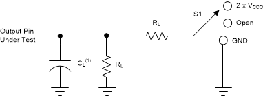
1. CL includes probe and jig capacitance.
Figure 2. Load CircuitTable 1. Loading Conditions for Parameter
| TEST | S1 |
|---|---|
| tPLH(3), tPHL(3) | Open |
| tPLZ(1), tPZL(2) | VLOAD |
| tPHZ(1), tPZH(2) | GND |
(1) tPLZ and tPHZ are the same as tdis.
(2) tPZL and tPZH are the same as ten.
(3) tPLH and tPHL are the same as tpd.
Table 2. Loading Conditions for VCC – Case 1
| VCC | INPUTS | VM | VLOAD | CL | RL | VΔ | |
|---|---|---|---|---|---|---|---|
| VI | tr/tf | ||||||
| 1.8 V ± 0.15 V | VCC | ≤ 2 ns | VCC / 2 | 2 × VCC | 15 pF | 1 MΩ | 0.15 V |
| 2.5 V ± 0.2 V | VCC | ≤ 2 ns | VCC / 2 | 2 × VCC | 15 pF | 1 MΩ | 0.15 V |
| 3.3 V ± 0.3 V | 3 V | ≤ 2.5 ns | 1.5 V | 6 V | 15 pF | 1 MΩ | 0.3 V |
| 5 V ± 0.5 V | VCC | ≤ 2.5 ns | VCC / 2 | 2 × VCC | 15 pF | 1 MΩ | 0.3 V |
Table 3. Loading Conditions for VCC – Case 2
| VCC | INPUTS | VM | VLOAD | CL | RL | VΔ | |
|---|---|---|---|---|---|---|---|
| VI | tr/tf | ||||||
| 1.8 V ± 0.15 V | VCC | ≤ 2 ns | VCC / 2 | 2 × VCC | 30 pF | 1 MΩ | 0.15 V |
| 2.5 V ± 0.2 V | VCC | ≤ 2 ns | VCC / 2 | 2 × VCC | 30 pF | 500 MΩ | 0.15 V |
| 3.3 V ± 0.3 V | 3 V | ≤ 2.5 ns | 1.5 V | 6 V | 30 pF | 500 MΩ | 0.3 V |
| 5 V ± 0.5 V | VCC | ≤ 2.5 ns | VCC / 2 | 2 × VCC | 30 pF | 500 MΩ | 0.3 V |
 Figure 3. Voltage Waveforms: Pulse Duration
1. The outputs are measured one at a time, with one transition per measurement.
Figure 4. Voltage Waveforms: Propagation Delay Times Inverting And Noninverting Outputs Figure 5. Voltage Waveforms: Setup and Hold Times
1. Waveform 1 is for an output with internal conditions such that the output is low, except when disabled by the output control.
2. Waveform 2 is for an output with internal conditions such that the output is high, except when disabled by the output control.
3. The outputs are measured one at a time, with one transition per measurement.
Figure 6. Voltage Waveforms: Enable and Disable Times, Low- and High-Level Enabling