SCBS778B November 2003 – June 2016 SN74LVTH16373-EP
PRODUCTION DATA.
- 1 Features
- 2 Applications
- 3 Description
- 4 Revision History
- 5 Pin Configuration and Functions
-
6 Specifications
- 6.1 Absolute Maximum Ratings
- 6.2 ESD Ratings
- 6.3 Recommended Operating Conditions
- 6.4 Thermal Information
- 6.5 Electrical Characteristics
- 6.6 Timing Requirements (I Version)
- 6.7 Switching Characteristics (I Version)
- 6.8 Timing Requirements (M Version)
- 6.9 Switching Characteristics (M Version)
- 6.10 Typical Characteristics
- 7 Parameter Measurement Information
- 8 Detailed Description
- 9 Application and Implementation
- 10Power Supply Recommendations
- 11Layout
- 12Device and Documentation Support
- 13Mechanical, Packaging, and Orderable Information
9 Application and Implementation
NOTE
Information in the following applications sections is not part of the TI component specification, and TI does not warrant its accuracy or completeness. TI’s customers are responsible for determining suitability of components for their purposes. Customers should validate and test their design implementation to confirm system functionality.
9.1 Application Information
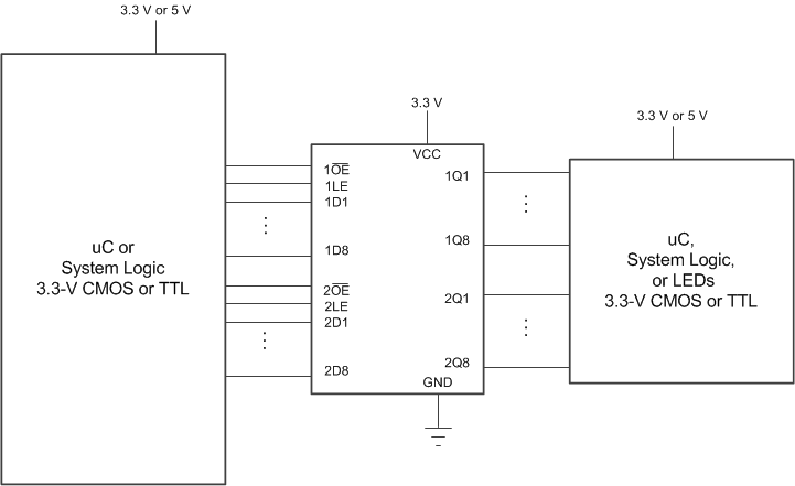
The specially designed 3-V LVTH family uses the 0.8-µ BiCMOS process technology for bus-interface functions. Like its 5-V ABT counterpart, LVHT provides up to 64 mA of drive, low propagation delays. The bus-hold feature eliminates requirements for external pullup resistors and I/Os that can handle up to 7 V, which allows them to act as 5-V/3-V translators.
9.2 Typical Application
 Figure 7. Application Diagram
9.2.1 Design Requirements
The SN54LVTH16373 utilizes BiCMOS technology with high-drive currents. Care must be taken to avoid bus contention that can disrupt system functionality and/or cause violation of absolute maximum ratings.
9.2.2 Detailed Design Procedure
- Recommended input conditions
- Rise time and fall time specifications. See Δt/ΔV in Recommended Operating Conditions.
- Specified high and low levels. See VIH and VIL in Recommended Operating Conditions.
- Inputs are overvoltage tolerant, which allows them to go as high as 5.5 V independent of VCC.
- Recommend output conditions
- Avoid buss contention.
- Do not exceed IOH and IOL current limits in Recommended Operating Conditions.
- Outputs that are being driven high may not be pulled above VCC by more they 0.5 V.
9.2.3 Application Curves
