ZHCSEP3B February 2016 – February 2016 THS3217
PRODUCTION DATA.
- 1 特性
- 2 应用
- 3 说明
- 4 修订历史记录
- 5 Device Comparison Table
- 6 Pin Configuration and Functions
-
7 Specifications
- 7.1 Absolute Maximum Ratings
- 7.2 ESD Ratings
- 7.3 Recommended Operating Conditions
- 7.4 Thermal Information
- 7.5 Electrical Characteristics: D2S
- 7.6 Electrical Characteristics: OPS
- 7.7 Electrical Characteristics: D2S + OPS
- 7.8 Electrical Characteristics: Midscale (DC) Reference Buffer
- 7.9 Typical Characteristics: D2S + OPS
- 7.10 Typical Characteristics: D2S Only
- 7.11 Typical Characteristics: OPS only
- 7.12 Typical Characteristics: Midscale (DC) Reference Buffer
- 7.13 Typical Characteristics: Switching Performance
- 7.14 Typical Characteristics: Miscellaneous Performance
- 8 Parameter Measurement Information
-
9 Detailed Description
- 9.1 Overview
- 9.2 Functional Block Diagram
- 9.3 Feature Description
- 9.4 Device Functional Modes
-
10Application and Implementation
- 10.1
Application Information
- 10.1.1
Typical Applications
- 10.1.1.1 High-Frequency, High-Voltage, Dual-Output Line Driver for AWGs
- 10.1.1.2 High-Voltage Pulse-Generator
- 10.1.1.3 Single-Supply, AC-Coupled, Piezo Element Driver
- 10.1.1.4 Output Common-Mode Control Using the Midscale Buffer as a Level Shifter
- 10.1.1.5 Differential I/O Driver With independent Common-Mode Control
- 10.1.1
Typical Applications
- 10.1
Application Information
- 11Power Supply Recommendations
- 12Layout
- 13器件和文档支持
- 14机械、封装和可订购信息
10 Application and Implementation
NOTE
Information in the following applications sections is not part of the TI component specification, and TI does not warrant its accuracy or completeness. TI’s customers are responsible for determining suitability of components for their purposes. Customers should validate and test their design implementation to confirm system functionality.
10.1 Application Information
10.1.1 Typical Applications
The five example designs presented show a good, but not comprehensive, range of the possible solutions that the THS3217 provides. Numerous more configurations are clearly possible to the creative designer.
10.1.1.1 High-Frequency, High-Voltage, Dual-Output Line Driver for AWGs
 Figure 95. Dual-Channel Design: 5 VPP at THS3217 Output and 20 VPP at THS3091 Output
10.1.1.1.1 Design Requirements
For this design example, use the parameters listed in Table 8 as the input parameters.
Table 8. Dual-Output Design Specifications
| DESIGN PARAMETER | EXAMPLE VALUE | |||
|---|---|---|---|---|
| High-frequency, THS3217 channel | 5-VPP, 100-MHz bandwidth | |||
| High-voltage, THS3091 channel | 20-VPP, 40-MHz bandwidth | |||
10.1.1.1.2 Detailed Design Procedure
The THS3217 is well suited for high-speed, low-distortion arbitrary waveform generator (AWG) applications commonly used in laboratory equipment. In this typical application, a high-speed, complementary-current-output DAC is used to drive the D2S. The OPS of the THS3217 easily drives a 100-MHz, 2.5-VPP signal into a matched 50-Ω load. When a larger output signal is required, consider using the THS3091 as the final driver stage.
A passive RLC filter is commonly used on DAC outputs to reduce the high-frequency content in the DAC steps. The filtering between the DAC output and the input to the D2S reduces higher-order DAC harmonics from feeding into the internal OPS path when the external input path is selected. Feedthrough between the internal and external OPS paths increases with increasing frequency; however, the input filter rolls off the DAC harmonics before the harmonics couple to VOUT (pin 10) through the deselected OPS signal path. Figure 96 shows an example of a doubly-terminated differential filter from the DAC to the THS3217 D2S inputs at pins 2 and 3.The DAC is modeled as two, fixed, 10-mA currents and a differential, ac-current source. The 10-mA dc midscale currents set up the average common-mode voltage at the DAC outputs and D2S inputs at 10 mA × 25 Ω = 0.25 VCM. The total voltage swing on the DAC outputs is 0 V to 0.5 V.
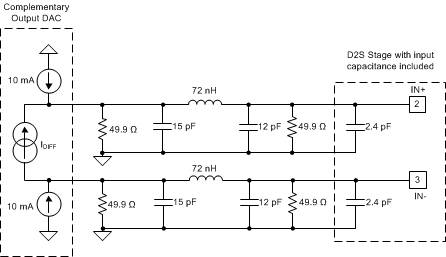 Figure 96. 200-MHz Butterworth Filter Between DAC and D2S Inputs
Some of the guidelines to consider in this filter design are:
- The filter cutoff is adjusted to hit a standard value in the standard high-frequency, chip inductors kits.
- The required filter output capacitance is reduced from the design value of 14.4 pF to 12 pF to account for the D2S input capacitance of 2.4 pF, as reported in the D2S Electrical Characteristics table.
- The capacitor at the DAC output pins must also be reduced by the expected DAC output pin capacitance. The DAC output capacitance is often specified as 5 pF, but is usually much lower. Contact the DAC manufacturer for an accurate value.
Figure 97 shows the TINA-simulated filter response for the input-stage filter. The low-frequency 34-dBΩ gain is due to the 50-Ω differential resistance at the DAC output terminals. At 400 MHz, this filter is down 16 dB from the 50-Ω level; it is also very flat through 100 MHz.
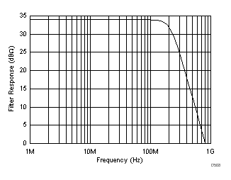 Figure 97. Simulated, Differential-Input Filter Response
In the example design of Figure 95, a 100-MHz, third-order Bessel filter is placed between the D2S output and the external OPS input. Another 50-MHz, third-order Bessel filter is placed at the input of a very-high, output-swing THS3091 stage. A double-pole, double-throw (DPDT) relay selects the THS3091 path when the internal OPS path is selected in the THS3217. Figure 95 shows this design. The key operational considerations in this design include:
- When the external OPS path is selected, the 2-VPP maximum D2S output swing experiences a 1.1-dB insertion loss from the interstage filter between VO1 (pin 6) and VIN+ (pin 9). A standard value inductor is used and the 255-Ω termination accounts for the internal 18.5-kΩ element. The 10-Ω resistor at pin 9 isolates the OPS input from the 52-pF filter capacitor. To recover the insertion loss and produce a maximum 5-VPP output, the OPS gain is set to 2.84 V/V. When the interstage filter path is selected, the two DPDT relays pass the OPS output on directly from the 49.9-Ω output matching resistor to VO, and the THS3091 can be disabled to conserve power.
- To deliver 20 VPP at the VO output, select the THS3091 path. Select the internal OPS path to bypass the 100-MHz filter (1.1-dB insertion loss) in order to give a maximum 5.7-VPP output at VOUT (pin 11). The two DPDT relays switch position, and the 49.9 Ω at the OPS output becomes part of the 50-MHz, third-order Bessel filter into the THS3091 stage. This filter has a 2-dB insertion loss requiring a gain of 4.4 V/V in the THS3091 to deliver 20 VPP from the OPS output.
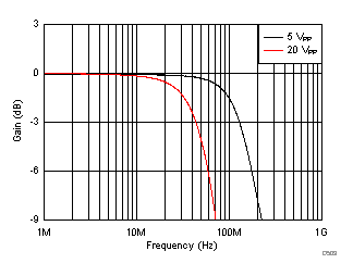
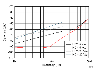
- Figure 98 and Figure 99 show the frequency response and harmonic distortion performance of the dual output-voltage system. The frequency response is normalized to 0 dB to make bandwidth comparisons easier.
10.1.1.1.3 Application Curves
10.1.1.2 High-Voltage Pulse-Generator
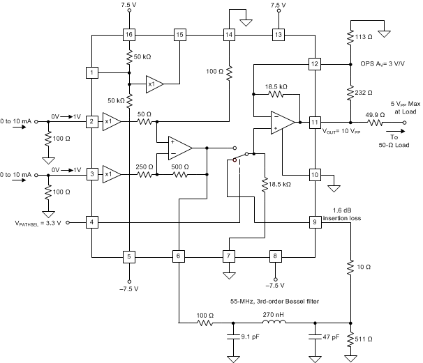 Figure 100. Driving a 10-VPP Pulse Output into a 100-Ω Load With a 55-MHz External Interstage Bessel Filter
10.1.1.2.1 Design Requirements
To design a high-voltage, high-speed pulse generator with minimum overshoot, use the parameters listed in Table 8 as the input parameters.
Table 9. Pulse-Generator Specifications
| DESIGN PARAMETER | EXAMPLE VALUE |
|---|---|
| Power supply | ±7.5 V |
| Pulse frequency | 10 MHz |
| Pulse output voltage | 10 VPP |
10.1.1.2.2 Detailed Design Procedure
Figure 100 shows an example design using the THS3217 to deliver a 10-VPP maximum voltage from a DAC input, and includes an example external, third-order, interstage Bessel filter. Some of the salient considerations for this design include:
- Reduced DAC output current with increased termination. This example is intended to be used with a current-sourcing DAC with an output compliance voltage of at least 1 V on a 0.5-V common-mode voltage. The 10-mA, single-ended, DAC tail current produces a 0-V to 1-V swing on each 100-Ω termination. The resulting 2-VPP differential DAC signal produces a higher SNR signal at the THS3217 inputs.
- The midscale buffer is not used. The VREF pin is grounded to set the inputs to a 4-VPP ground-centered maximum output swing at VO1 (pin 6). The external input to the OPS is selected by setting PATHSEL to 3.3 V (anything over 1.3 V is adequate, or tie this pin to +VCC for fixed, external-path operation).
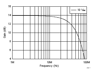
- The interstage Bessel filter is –0.3-dB flat through 20 MHz, with only 1.6 dB of insertion loss. The filter is designed to be low insertion-loss with relatively high resistor values. The filter uses standard inductor values. The capacitors are also standard-value, and slightly off from the exact filter solution. The final resistor to ground is designed for 500 Ω, but increased here to a standard 511 Ω externally to account for the internal 18.5-kΩ resistor on the external OPS input pin to GND. To isolate the last 47-pF filter capacitor from the OPS input stage, a 10-Ω series resistor is added close to the pin 9 input.
- The filter adds 1.6 dB of insertion loss that is recovered, to achieve a 10-VPP maximum output by designing the OPS for a gain of 3 V/V. Looking at Table 7, this gain setting requires the 232-Ω external RF and 113-Ω RG to ground for best operation.
- For 10-VPP maximum output, using the ±7.5-V supplies shown here gives adequate headroom in the OPS output stage. The operating maximum supply of 15.8 V requires a 5% tolerance on these ±7.5-V supplies.
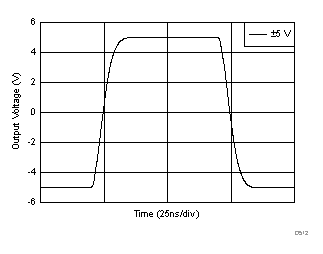
- The Bessel filter gives a very low overshoot full-scale output step-response, as shown in the 10-MHz, ±5-V square wave of Figure 102. The frequency response of the system is shown in Figure 101.
10.1.1.2.3 Application Curves
10.1.1.3 Single-Supply, AC-Coupled, Piezo Element Driver
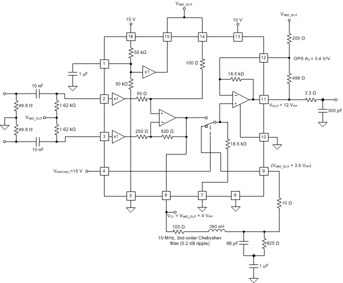 Figure 103. Single-Supply, Heavy Capacitive-Load Driving
10.1.1.3.1 Design Requirements
The very-high peak output current and slew rate of the THS3217 OPS make it particularly suitable for driving heavy capacitive loads, such as the piezo elements used in continuous wave (CW) applications that require high-amplitude, sinusoidal-type excitations. The driver is quickly disabled during the receive time when the output TR switch is moved to receive mode. Figure 103 shows an example design using the internal midscale buffer to bias all the stages to midsupply on a single 15-V design. There are many elements to this example that also apply to any single-supply application. The key points here are:
- The differential DAC input signal is ac-coupled to the D2S input, and the termination resistors are scaled up and biased to midsupply using the output of the midscale buffer, VMID_OUT (pin 15). The 10-nF blocking capacitors before the 1.62 kΩ termination resistors set the high-pass pole at 10 kHz.
- The internal divider resistors of the midscale buffer are decoupled using a 1-µF capacitor on VMID_IN (pin 1). Use of the capacitor improves both noise and PSRR through the reference buffer stage. In turn, the noise injected by the bias source is reduced at the various places the buffer output is used.
- VMID_OUT is also applied to the VREF input (pin 14) to hold the D2S output centered on the single 15-V supply. There is minimal dc current into VREF (pin 14) because the D2S input buffers operate at the same common-mode voltage, VMID_OUT.
- The D2S output is dc biased at midsupply and delivers two times the differential swing applied at its inputs. Assuming 2 VPP at the D2S inputs implies 4 VPP at the D2S output pins. Lower input swings are supported with the gain in the OPS adjusted to meet the desired output maximum.
- The filter in Figure 103 is a 0.2-dB ripple, second-order Chebyshev filter at 15 MHz. If the desired maximum frequency is 12 MHz, for instance, this filter is attenuating the HD2 and HD3 out of the D2S by approximately 3 dB and 5 dB, respectively. Increased attenuation can be provided with higher-order filters, but this simple filter does a good job of band-limiting the high-frequency noise from the D2S outputs before the noise gets into the OPS stage.
- The dc bias voltage at VO1 drives a small dc current into the 18.5-kΩ resistor to ground at the OPS external input, VIN+ (pin 9). The error voltage due to the bias current will level-shift the dc voltage at the OPS noninverting input through the 105-Ω filter resistor. This offset will be amplified by the OPS gain since its RG element is referenced to the VMID output with a dc gain of 3.4 V/V.
- The logic lines are still referenced to ground in this single-supply application. The external path to the OPS is selected by connecting PATHSEL (pin 4) to +VCC. DISABLE (pin 10) is grounded in this example in order to hold the OPS on. If the disable feature is required by the application, drive the OPS using a standard logic control driver. Note that the midscale buffer output still drives RG and RF to midsupply in this configuration with the OPS disabled.
- The RG element can be ac coupled to ground through a capacitor to operate at midsupply. Figure 103 shows the midscale buffer driving RG, thus eliminating the need for an added capacitor. Using a blocking capacitor moves the dc gain to 1 V/V. The voltage on the external, noninverting input of the OPS sets the dc operating point. Use of a blocking capacitor also lightens the load on the midscale buffer output, and eliminates the bias on RG when the OPS is disabled.
- Piezo element drivers operate in a relatively low-frequency range; therefore, the OPS RF is scaled up even further than the values suggested in Table 7. An increased RF allows RG to also be scaled up, thereby reducing the load on the midscale buffer, and allow a lower series output resistor to be used into the 300-pF capacitive load.
- The peak charging current into the capacitive load occurs at the peak dV/dT point. Assuming a 12-MHz sinusoid at 12 VPP requires a peak output current from the OPS of 6 VPEAK × 2π × 12 MHz × 300 pF = 135 mA. This result matches the rated minimum peak output current of the OPS.
Using a very low series resistor limits the waveform distortion due to the I × R drop at the peak charging point around the sinusoidal zero crossing. The 135 mA through 3.3 Ω causes a 0.45-V peak drop to the load capacitance around zero crossing. The voltage drop across the series output resistor increases the apparent third harmonic distortion at the capacitive load. Figure 45 and Figure 46 show 10-VPP distortion sweeps into various capacitor loads. The results shown in these figures are for the OPS only because the results set the harmonic distortion performance in this example.
10.1.1.4 Output Common-Mode Control Using the Midscale Buffer as a Level Shifter
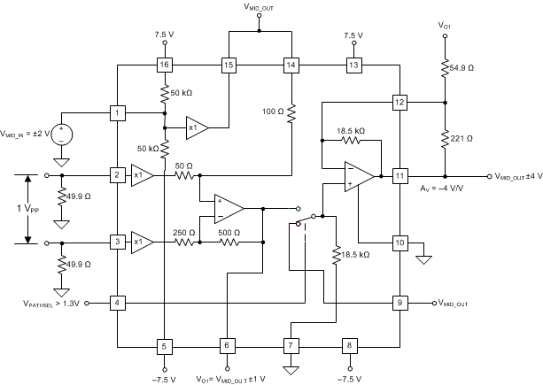 Figure 104. Adding an Output DC Offset Using the Midscale Buffer
10.1.1.4.1 Design Requirements
An easy way to insert a dc offset into the signal channel (without sacrificing any of the DAC dynamic range) is to apply the desired offset at VMID_IN and use it to bias VREF (pin 14) and VIN+ (pin 9). An example is shown in Figure 104. This example shows a relatively low maximum differential input of 1 VPP on any compliance voltage required by the DAC. Other configuration options include:
- The D2S output is offset using a dc input at VMID_IN (pin 1). Although shown here as ±2 V, the dc offset expands to ±3.5 V when using ±7.5-V supplies.
- Connecting VMID_OUT to the VREF input places the D2S output at the dc offset voltage along with a gain of 2 V/V version of the differential input voltage. The stated range of ±2 V, along with the ±0.5 V out of the upper input buffer, requires a peak output current from VMID_OUT of 2.5 V / 150 Ω = 16.7 mA. This value is well below the rated minimum linear output current of 40 mA.
- The dc offset voltage is then applied to the external OPS input. Connecting the circuit in this manner results in no additional dc gain between the D2S and OPS outputs, while it continues to retain the signal gain of the OPS configured as an inverting amplifier. The values of RF and RG in this application example are derived from Table 4. The OPS is setup for a gain of –4 V/V in this example. Using the resistor values from Table 4 results in the widest bandwidth for the OPS; however, the RG = 54.9 Ω resistor presents a heavy load to the D2S output. In such cases, scaling up the resistors in the OPS helps reduce the loading on the D2S output at the expense of reduced OPS bandwidth.
- No filtering is shown in this example; however, introducing filtering in the OPS RG path is certainly possible. In such cases, the RG element is also the filter termination resistor. Any filtering adds some insertion loss that can be recovered in the OPS stage.
10.1.1.5 Differential I/O Driver With independent Common-Mode Control
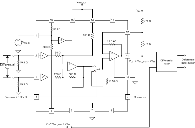 Figure 105. Differential I/O Line Driver
10.1.1.5.1 Design Requirements
Certain applications require the differential DAC output voltage to be level-translated from one common-mode (compliance) level to a differential output at a different common-mode level. The THS3217 performs this function directly using the very flexible blocks provided internally. Figure 105 shows an example of such an application, where the differential gain is always 4 V/V. The differential gain is fine-tuned down by setting the insertion loss in the differential post-filter. The considerations critical to this application include:
- The input is dc-coupled with the appropriate termination impedance required by the DAC. Use a high-frequency, antialiasing filter at the input to limit DAC feedthrough in the deselected OPS internal input.
- The output common-mode control is set with the voltage applied to the VMID buffer input at VMID_IN (pin 1). The circuit is configured so that the output at VMID_OUT (pin 15) drives both VREF (pin 14), in order to set the D2S dc output voltage, and VIN+ (pin 9).
- The D2S output available at VO1 (pin 6) provides one side of the differential-output, and is dc-biased at VMID_OUT. This VO1 also drives the RG resistor for the OPS in an inverting gain of –1 V/V. The dc bias level at the RG input and the V+ input of the OPS are the same voltage; therefore, no level shift through the OPS occurs. The OPS outputs an inverted version of the D2S output signal at the same common-mode voltage (VMID_OUT). The wideband, differential signal with independent output common-mode voltage control can now be applied to a differential filter and on to the next stage.
- Make sure that the differential filter only has differential resistors and capacitors. Termination resistors to ground level shift the input common-mode voltage, while differential resistors transfers the desired VMID_OUT directly through the filter.
- If the desired VMID_OUT + differential signal combined clips in the OPS or D2S stages, offset the supplies to gain headroom. For instance, if a 5-V output common-mode voltage is required with a 10-VPP differential signal, the OPS and D2S must deliver 2.5-V to 7.5-V output swings. The D2S has the higher headroom requirement at 1.55 V (max). Operating the THS3217 with –5 V and +10 V supplies stays within the rated maximum of 15.8 V total supply range, and provide adequate headroom for the positive offset swing requirement. Note that the logic lines are still referenced to GND by pin 7. Tying PATHSEL (pin 4) to +VCC holds this design in the external path mode required.