ZHCSDZ2A February 2013 – July 2015 THS4532
PRODUCTION DATA.
- 1 特性
- 2 应用
- 3 说明
- 4 修订历史记录
- 5 Related Products
- 6 Pin Configuration and Functions
- 7 Specifications
- 8 Detailed Description
-
9 Application and Implementation
- 9.1
Application Information
- 9.1.1 Frequency Response and Output Impedance
- 9.1.2 Distortion
- 9.1.3 Slew Rate, Transient Response, Settling Time, Overdrive, Output Voltage, and Turnon and Turnoff Time
- 9.1.4 Common-Mode and Power Supply Rejection
- 9.1.5 VOCM Input
- 9.1.6 Balance Error
- 9.1.7 Single-Supply Operation
- 9.1.8 Low-Power Applications and the Effects of Resistor Values on Bandwidth
- 9.1.9 Driving Capacitive Loads
- 9.1.10 Audio Performance
- 9.1.11 Audio On and Off Pop Performance
- 9.2 Typical Applications
- 9.3 Systems Examples
- 9.1
Application Information
- 10Power Supply Recommendations
- 11Layout
- 12器件和文档支持
- 13机械、封装和可订购信息
8 Detailed Description
8.1 Overview
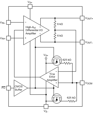
As shown in the Functional Block Diagram, the THS4532 device is comprised of three functional blocks: a fully-differential amplifier with high open-loop gain of 114 dB, a servo amplifier to set the common-mode voltage of the output equal to the VOCM input, and a power-down circuit to greatly reduce the power consumption when the device is idle.
The common-mode voltage servo has impressive performance specifications of ±1% maximum gain error, ±5-mV maximum voltage offset, and 24-MHz bandwidth.
8.2 Functional Block Diagram

8.3 Feature Description
8.3.1 Input Common-Mode Voltage Range
The input common-mode voltage of a fully-differential amplifier is the voltage at the positive and negative (+ and –) input pins of the amplifier.
Do not violate the input common-mode voltage range (VICR) of the amplifier. Assuming the amplifier is in linear operation, the voltage across the input pins is only a few millivolts at most. Therefore, finding the voltage at one input pin determines the input common-mode voltage of the amplifier.
Use Equation 1 to calculate the voltage with the negative input as a summing node.

To determine the VICR of the amplifier, the voltage at the negative input is evaluated at the extremes of VOUT+.
As the gain of the amplifier increases, the input common-mode voltage becomes closer and closer to the input common-mode voltage of the source.
8.3.1.1 Setting the Output Common-Mode Voltage
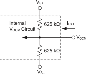
The output common-model voltage is set by the voltage at the VOCM pin and the internal circuit works to maintain the output common-mode voltage as close as possible to this voltage. If left unconnected, the output common-mode is set to mid-supply by internal circuitry, which may be over-driven from an external source. Figure 69 is representative of the VOCM input. The internal VOCM circuit has about 24-MHz of –3-dB bandwidth, which is required for best performance, but it is intended to be a DC bias input pin. Bypass capacitors are recommended on this pin to reduce noise. Use Equation 2 to calculate the external current required to overdrive the internal resistor divider.

where
- VOCM is the voltage applied to the VOCM pin.
 Figure 69. Simplified VOCM Input Circuit
8.3.2 Power Down
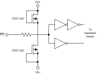
The power down pin is internally connected to a CMOS stage which must be driven to a minimum of 2.1 V to ensure proper high logic.
 Figure 70. Simplified Power-Down Internal Circuit
If 1.8-V logic is used to drive the pin, a shoot through current of up to 100 µA may develop in the digital logic causing the overall quiescent current to exceed the 2 µA of maximum disabled quiescent current specified in the Electrical Characteristics: VS = 2.7 V.
To properly interface to 1.8-V logic with minimal increase in additional current draw, a logic-level translator like the SN74AVC1T45 device can be used.
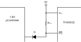
Alternatively, the same function can be achieved using a diode and pullup resistor as shown in Figure 71.
 Figure 71. THS5432 Power Down Interface to 1.8-V Logic Microcontroller
The voltage at the power down pin will be a function of the supply voltage, input logic level, and diode drop. As long as the diode is forward biased, the power down voltage is calculated using Equation 3.

where
- VL is the logic level voltage.
- Vf is the forward voltage drop across the diode.
This means for 1.8-V logic, the forward voltage of the diode should be greater than 0.3 V but less than 0.7 V to keep the power down logic level above 2.1 V and less than 0.7 V respectively.
For example, if 1N914 is selected as the diode with a forward voltage of approximately 0.4 V, the translated logic voltages will be 0.4 V for disabled operation and 2.2 V for enabled operation.
Use Equation 4 to calculate the additional current draw.

Equation 2 shows that larger values of RPU result in a smaller additional current. A reasonable value of RPU is 500 kΩ where an additional current draw of 5.2 µA is expected while the device is in operation and 1.6 µA when disabled.
8.4 Device Functional Modes
The THS4532 has two functional modes: full-power mode and power-down mode. The power-down mode reduces the quiescent current of the device to 500 nA from a typical value of 290 µA with a 5-V supply.
With a turnon time of only 600 ns and a turnoff time of 15 ns, the power-down mode can be used to greatly reduce the average power consumption of the device without sacrificing system performance.