ZHCSGR2D August 2017 – February 2021 THS4561
PRODUCTION DATA
- 1 特性
- 2 应用
- 3 说明
- 4 Revision History
- 5 Device Comparison Table
- 6 Pin Configuration and Functions
-
7 Specifications
- 7.1 Absolute Maximum Ratings
- 7.2 ESD Ratings
- 7.3 Recommended Operating Conditions
- 7.4 Thermal Information
- 7.5 Electrical Characteristics: VS+ – VS– = 5 V to 12 V
- 7.6 Typical Characteristics: (VS+) – (VS–) = 12 V
- 7.7 Typical Characteristics: (VS+) – (VS–) = 5 V
- 7.8 Typical Characteristics: (VS+) – (VS–) = 3 V
- 7.9 Typical Characteristics: (VS+) – (VS–) = 3-V to 12-V Supply Range
-
8 Parameter Measurement Information
- 8.1 Example Characterization Circuits
- 8.2 Output Interface Circuit for DC-Coupled Differential Testing
- 8.3 Output Common-Mode Measurements
- 8.4 Differential Amplifier Noise Measurements
- 8.5 Balanced Split-Supply Versus Single-Supply Characterization
- 8.6 Simulated Characterization Curves
- 8.7 Terminology and Application Assumptions
- 9 Detailed Description
- 10Application and Implementation
- 11Power Supply Recommendations
- 12Layout
- 13Device and Documentation Support
- 14Mechanical, Packaging, and Orderable Information
封装选项
机械数据 (封装 | 引脚)
散热焊盘机械数据 (封装 | 引脚)
订购信息
10.2 Typical Application
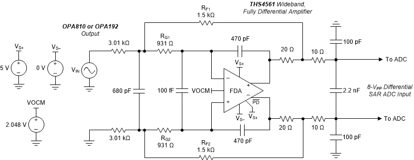
One common application for the THS4561 is to take a single-ended, high VPP voltage swing (from a high-voltage precision amplifier such as the OPA810 or OPA192) and deliver that swing to precision SAR ADC as a single-ended to differential conversion with output common-mode control and implement an active 2nd-order multiple feedback (MFB) filter design. Designing for a 16-VPP maximum input down to an 8-VPP differential swing requires a gain of 0.5 V/V. Targeting a 170-kHz Butterworth response with the RC elements tilted towards low noise gives the example design of Figure 10-7. The VCM control is set to half of a 4.096-V reference, which is typical for
5-V differential SAR applications. With the high voltage capabilities of the THS4561, the design can be easily adopted for 20-VPP input swing to the FDA for a full 10-VPP swing into 5-V differential SAR ADC by simply using wider power supplies for the THS4561 to allow for increased output swing headroom with minimal performance degradation.
 Figure 10-7 MFB Filter Driving an ADC
Application:
 Example 170-kHz Butterworth Response