ZHCSH83 December   2017 TLV2172-Q1

PRODUCTION DATA.  

  1. 特性
  2. 应用
  3. 说明
    1.     简化电路原理图
  4. 修订历史记录
  5. Pin Configuration and Functions
    1.     Pin Functions
  6. Specifications
    1. 6.1 Absolute Maximum Ratings
    2. 6.2 ESD Ratings
    3. 6.3 Recommended Operating Conditions
    4. 6.4 Thermal Information: TLV2172-Q1
    5. 6.5 Electrical Characteristics
    6. 6.6 Typical Characteristics
  7. Detailed Description
    1. 7.1 Overview
    2. 7.2 Functional Block Diagram
    3. 7.3 Feature Description
      1. 7.3.1 Operating Characteristics
      2. 7.3.2 Phase-Reversal Protection
      3. 7.3.3 Electrical Overstress
      4. 7.3.4 Capacitive Load and Stability
    4. 7.4 Device Functional Modes
      1. 7.4.1 Common-Mode Voltage Range
      2. 7.4.2 Overload Recovery
  8. Application and Implementation
    1. 8.1 Application Information
    2. 8.2 Typical Application
      1. 8.2.1 Design Requirements
      2. 8.2.2 Detailed Design Procedure
      3. 8.2.3 Application Curve
  9. Power Supply Recommendations
  10. 10Layout
    1. 10.1 Layout Guidelines
    2. 10.2 Layout Example
  11. 11器件和文档支持
    1. 11.1 器件支持
      1. 11.1.1 Third-Party Products Disclaimer
      2. 11.1.2 开发支持
        1. 11.1.2.1 TINA-TI™(免费软件下载)
        2. 11.1.2.2 DIP 适配器 EVM
        3. 11.1.2.3 通用运放 EVM
        4. 11.1.2.4 TI 高精度设计
        5. 11.1.2.5 WEBENCH滤波器设计器
    2. 11.2 文档支持
      1. 11.2.1 相关文档
    3. 11.3 相关链接
    4. 11.4 接收文档更新通知
    5. 11.5 社区资源
    6. 11.6 商标
    7. 11.7 静电放电警告
    8. 11.8 Glossary
  12. 12机械、封装和可订购信息

封装选项

机械数据 (封装 | 引脚)
散热焊盘机械数据 (封装 | 引脚)
订购信息

Capacitive Load and Stability

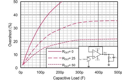
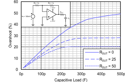
The dynamic characteristics of the TLV2172-Q1 are optimized for common operating conditions. The combination of low closed-loop gain and high capacitive loads decreases the phase margin of the amplifier and can lead to gain peaking or oscillations. As a result, heavier capacitive loads must be isolated from the output. The simplest way to achieve this isolation is to add a small resistor (for example, ROUT equal to 50 Ω) in series with the output. Figure 27 and Figure 28 show graphs of small-signal overshoot versus capacitive load for several values of ROUT. See the Feedback Plots Define Op Amp AC Performance application note for details of analysis techniques and application circuits.
TLV2172-Q1 C022_correct_graph_SBOS618.gif
100-mV output step, G = –1
Figure 27. Small-Signal Overshoot vs Capacitive Load
TLV2172-Q1 D023_SBOS784_correct_graph.gif
100-mV output step, G = 1
Figure 28. Small-Signal Overshoot vs Capacitive Load