ZHCSMR5 November 2020 TLV6703-Q1
PRODUCTION DATA
- 1 特性
- 2 应用
- 3 说明
- 4 Revision History
- 5 Device Comparison Table
- 6 Pin Configuration and Functions
- 7 Specifications
- 8 Detailed Description
- 9 Application and Implementation
- 10Power-Supply Recommendations
- 11Layout
- 12Device and Documentation Support
- 13Mechanical, Packaging, and Orderable Information
7.9 Typical Characteristics
at TJ = 25°C and VDD = 5 V (unless otherwise noted)
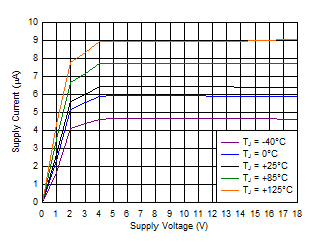 Figure 7-2 Supply Current (IDD) vs Supply Voltage (VDD)
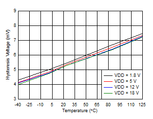 Figure 7-4 Hysteresis (Vhys) vs Temperature
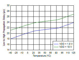
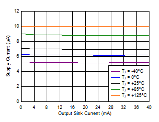 Figure 7-8 Supply Current (IDD) vs Output Sink Current
 Figure 7-10 Output Voltage Low (VOL) vs Output Sink Current (0°C)
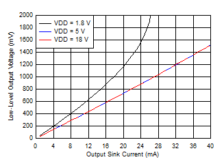 Figure 7-12 Output Voltage Low (VOL) vs Output Sink Current (85°C)
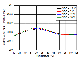 Figure 7-3 Rising Input Threshold Voltage (VIT+) vs Temperature
 Figure 7-5 Propagation Delay vs Temperature (High-to-Low Transition at Sense)
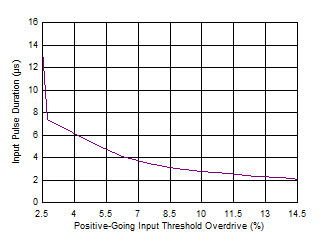
| SENSE = negative spike below VIT– |
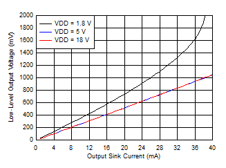 Figure 7-9 Output Voltage Low (VOL) vs Output Sink Current (–40°C)
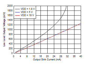 Figure 7-11 Output Voltage Low (VOL) vs Output Sink Current (25°C)
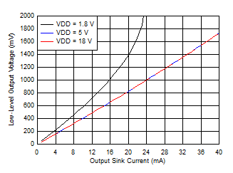 Figure 7-13 Output Voltage Low (VOL) vs Output Sink Current (125°C)