ZHCSA82F September   2012  – August 2019 TLV713

PRODUCTION DATA.  

  1. 特性
  2. 应用
  3. 说明
    1.     Device Images
      1.      典型应用电路
      2.      压降电压与输出电流间的关系
  4. 修订历史记录
  5. Pin Configurations and Functions
    1.     Pin Functions
  6. Specifications
    1. 6.1 Absolute Maximum Ratings
    2. 6.2 ESD Ratings
    3. 6.3 Recommended Operating Conditions
    4. 6.4 Thermal Information
    5. 6.5 Electrical Characteristics
    6. 6.6 Typical Characteristics
  7. Detailed Description
    1. 7.1 Overview
    2. 7.2 Functional Block Diagrams
    3. 7.3 Feature Description
      1. 7.3.1 Undervoltage Lockout (UVLO)
      2. 7.3.2 Shutdown
      3. 7.3.3 Foldback Current Limit
      4. 7.3.4 Thermal Protection
    4. 7.4 Device Functional Modes
      1. 7.4.1 Normal Operation
      2. 7.4.2 Dropout Operation
      3. 7.4.3 Disabled
  8. Application and Implementation
    1. 8.1 Application Information
      1. 8.1.1 Input and Output Capacitor Considerations
      2. 8.1.2 Dropout Voltage
      3. 8.1.3 Transient Response
      4. 8.1.4 UVLO Circuit Limitation
    2. 8.2 Typical Application
      1. 8.2.1 Design Requirements
      2. 8.2.2 Detailed Design Procedure
      3. 8.2.3 Application Curves
    3. 8.3 What to Do and What Not to Do
  9. Power Supply Recommendations
  10. 10Layout
    1. 10.1 Layout Guidelines
      1. 10.1.1 Board Layout Recommendations to Improve PSRR and Noise Performance
      2. 10.1.2 Power Dissipation
    2. 10.2 Layout Examples
  11. 11器件和文档支持
    1. 11.1 器件支持
      1. 11.1.1 开发支持
        1. 11.1.1.1 评估模块
        2. 11.1.1.2 Spice 模型
      2. 11.1.2 器件命名规则
    2. 11.2 文档支持
      1. 11.2.1 相关文档
    3. 11.3 接收文档更新通知
    4. 11.4 社区资源
    5. 11.5 商标
    6. 11.6 静电放电警告
    7. 11.7 Glossary
  12. 12机械、封装和可订购信息

封装选项

机械数据 (封装 | 引脚)
散热焊盘机械数据 (封装 | 引脚)
订购信息

Pin Configurations and Functions

DQN Package
4-Pin X2SON
Top View
TLV713 po_dfn_dpw_bvs195.gif
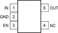
DBV Package
5-Pin SOT-23
Top View
TLV713 po_sot23_bvs195.gif

Pin Functions

PIN I/O DESCRIPTION
NAME NO.
X2SON SOT-23
EN 3 3 I Enable pin. Driving EN over 0.9 V turns on the regulator.
Driving EN below 0.4 V puts the regulator into shutdown mode.
GND 2 2 Ground pin
IN 4 1 I Input pin. A small capacitor is recommended from this pin to ground. See the Input and Output Capacitor Considerations section in the Feature Description for more details.
NC 4 No internal connection
OUT 1 5 O Regulated output voltage pin. For best transient response, a small 1-μF ceramic capacitor is recommended from this pin to ground. See the Input and Output Capacitor Considerations section in the Feature Description for more details.
Thermal pad The thermal pad is electrically connected to the GND node. Connect to the GND plane for improved thermal performance.