ZHCSL40M November 2004 – January 2023 TLVH431 , TLVH431A , TLVH431B , TLVH432 , TLVH432A , TLVH432B
PRODUCTION DATA
- 1 特性
- 2 应用
- 3 说明
- 4 Revision History
- 5 Pin Configuration and Functions
- 6 Specifications
- 7 Parameter Measurement Information
- 8 Detailed Description
- 9 Applications and Implementation
- 10Power Supply Recommendations
- 11Layout
- 12Device and Documentation Support
- 13Mechanical, Packaging, and Orderable Information
封装选项
机械数据 (封装 | 引脚)
散热焊盘机械数据 (封装 | 引脚)
- PK|3
订购信息
6.8 Typical Characteristics
Operation of the device at these or any other conditions beyond those indicated in the GUID-04CA6D15-7338-4464-8D24-EDF285F2DACF.html#GUID-04CA6D15-7338-4464-8D24-EDF285F2DACF table are not implied.
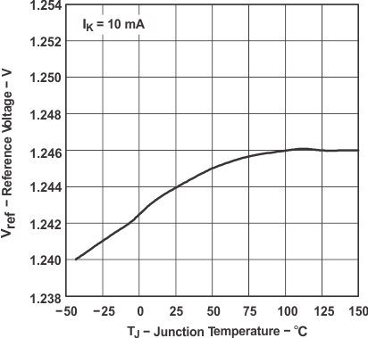 Figure 6-1 Reference Voltage vs Junction Temperature
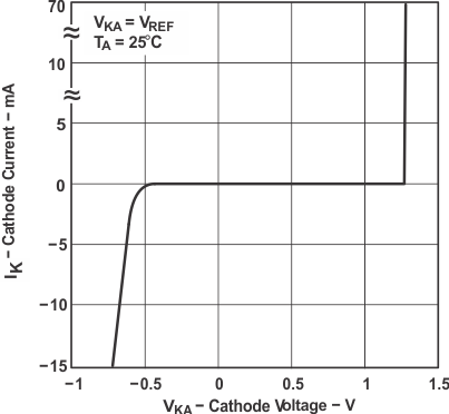 Figure 6-3 Cathode Current vs Cathode Voltage
 Figure 6-5 Minimum Cathode Current vs. Temperature
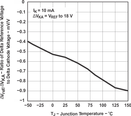
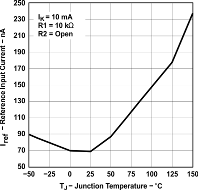
 Figure 6-4 Cathode Current vs Cathode Voltage
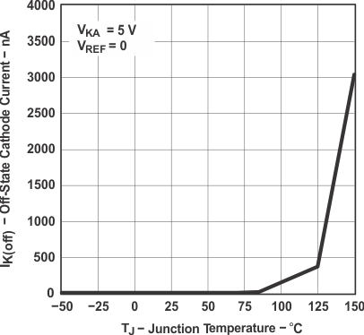 Figure 6-6 Off-State Cathode Current vs Junction Temperature
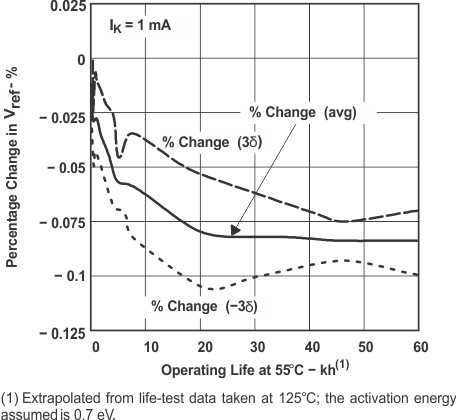 Figure 6-8 Percentage Change in VREF vs Operating Life at 55°C
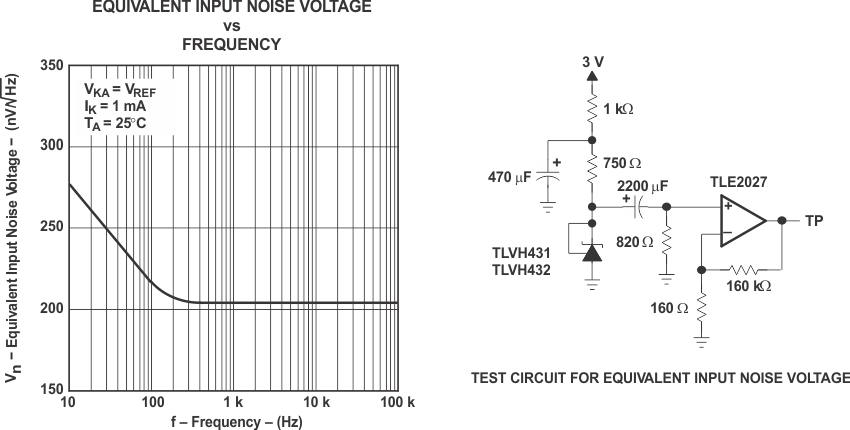 Figure 6-9 Equivalent Input Noise Voltage
 Figure 6-11 Voltage Gain and Phase Margin
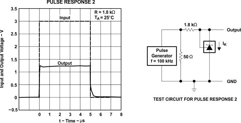 Figure 6-13 Pulse Response 2
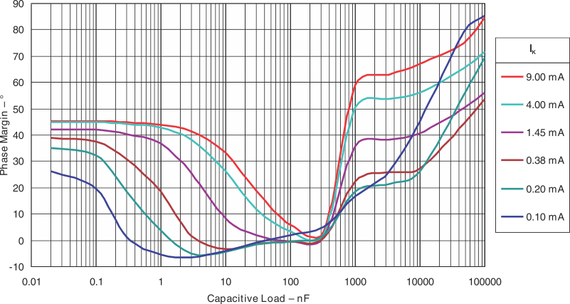 Figure 6-15 Phase Margin vs Capacitive Load VKA = VREF (1.25 V), TA= 25°C
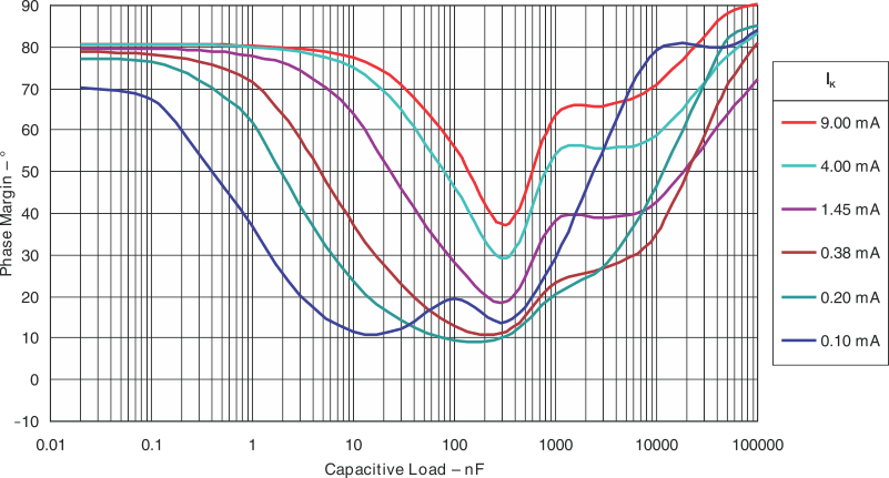 Figure 6-17 Phase Margin vs Capacitive Load VKA = 5.00 V, TA= 25°C
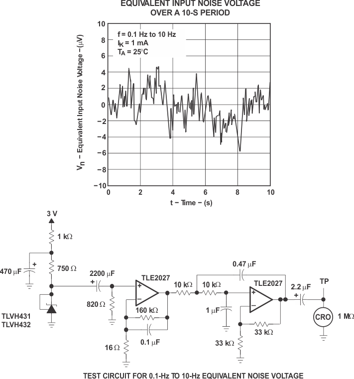
 Figure 6-12 Pulse Response 1
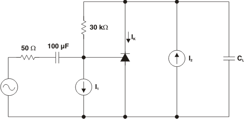 Figure 6-14 Phase Margin Test Circuit
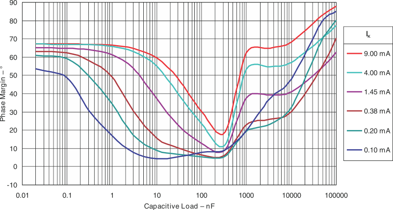 Figure 6-16 Phase Margin vs Capacitive Load VKA = 2.50 V, TA= 25°C