ZHCS246E May 2011 – April 2015 TMP006
PRODUCTION DATA.
- 1 特性
- 2 应用
- 3 说明
- 4 修订历史记录
- 5 Device Comparison Table
- 6 Pin Configuration and Functions
- 7 Specifications
-
8 Detailed Description
- 8.1 Overview
- 8.2 Functional Block Diagram
- 8.3 Feature Description
- 8.4 Device Functional Modes
- 8.5 Register Maps
- 9 Application and Implementation
- 10Power-Supply Recommendations
- 11Layout
- 12器件和文档支持
- 13机械、封装和可订购信息
11 Layout
11.1 Layout Guidelines
The IR thermopile sensor in the TMP006 and TMP006B is as susceptible to conducted and radiant IR energy from below the sensor on the PCB as it is to the IR energy from objects in its forward-looking field of view. When the area of PCB below the TMP006 or TMP006B is at the same temperature as the die or substrate of the TMP006 or TMP006B, heat is not transferred between the IR sensor and the PCB. However, temperature changes on a closely-placed target object or other events that lead to changes in system temperature can cause the PCB temperature and the TMP006 or TMP006B temperature to drift apart from each other. This drift in temperatures can cause a heat transfer between the IR sensor and the PCB to occur. Because of the small distance between the PCB and the bottom of the sensor, this heat energy will be conducted (as opposed to radiated) through the thin layer of air between the IR sensor and the PCB below it. This heat conduction causes offsets in the IR sensor voltage readings and ultimately leads to temperature calculation errors. To prevent and minimize these errors, the TMP006 and TMP006B layouts must address critical factors:
Thermally isolate the TMP006 and TMP006B from the rest of the PCB and any heat sources on it. Provide a stable thermal environment to reduce the noise in the measurement readings
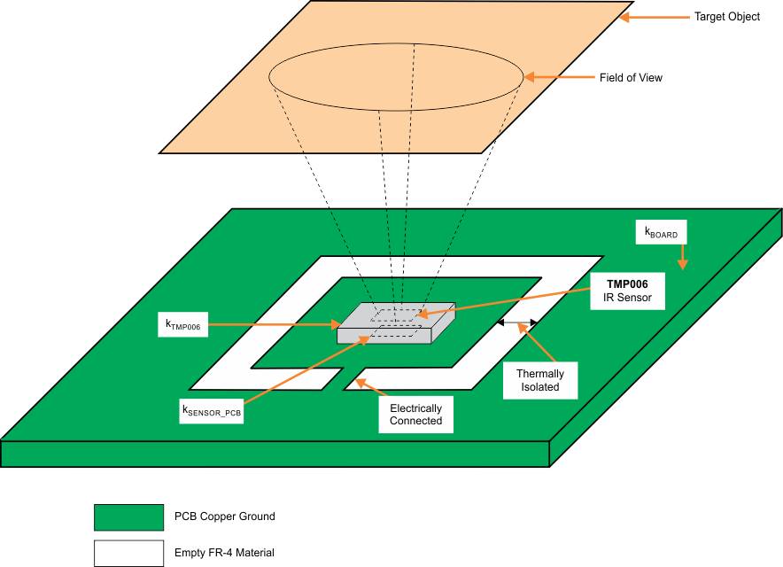
Figure 22 illustrates the concept of thermally isolating the TMP006 and TMP006B from the PCB and external heat sources such as other components, air currents, and so on.
 Figure 22. Principle of TMP006 and TMP006B Thermal Isolation
11.2 Layout Examples
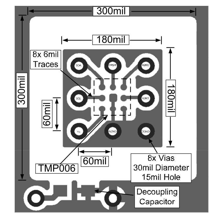
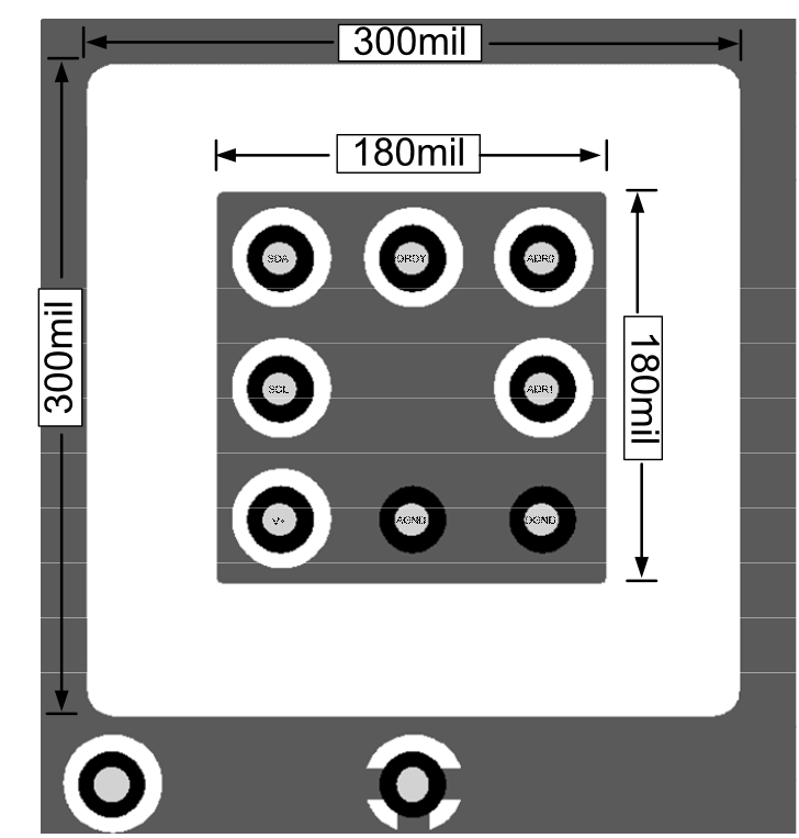
For more detailed information, refer to SBOU108 — TMP006 Layout and Assembly Guidelines.
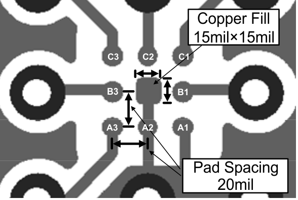
Use a 12-mil pad and 15-mil solder balls for A1, A2, A3, B1, B3, C1, C2 and C3.


