ZHCSAV1A April   2013  – September 2019 TMP108

PRODUCTION DATA.  

  1. 特性
  2. 应用
  3. 说明
    1.     Device Images
      1.      方框图
  4. 修订历史记录
  5. Pin Configuration and Functions
    1.     Pin Functions
  6. Specifications
    1. 6.1 Absolute Maximum Ratings
    2. 6.2 ESD Ratings
    3. 6.3 Recommended Operating Conditions
    4. 6.4 Thermal Information
    5. 6.5 Electrical Characteristics
    6. 6.6 Timing Diagrams
      1. 6.6.1 Two-Wire Timing Diagrams
    7. 6.7 Typical Characteristics
  7. Detailed Description
    1. 7.1 Overview
    2. 7.2 Functional Block Diagram
    3. 7.3 Feature Description
      1. 7.3.1 Serial Interface
      2. 7.3.2 Serial Bus Address
      3. 7.3.3 Bus Overview
      4. 7.3.4 Writing and Reading Operation
      5. 7.3.5 Slave Mode Operations
        1. 7.3.5.1 Slave Receiver Mode:
        2. 7.3.5.2 Slave Transmitter Mode:
      6. 7.3.6 SMBus Alert Function
      7. 7.3.7 General Call
      8. 7.3.8 High-Speed (Hs) Mode
      9. 7.3.9 Timeout Function
    4. 7.4 Device Functional Modes
      1. 7.4.1 Shutdown Mode (M1 = 0, M0 = 0)
      2. 7.4.2 One-Shot Mode (M1 = 0, M0 = 1)
      3. 7.4.3 Continuous Conversion Mode (M1 = 1)
    5. 7.5 Programming
      1. 7.5.1 Pointer Register
      2. 7.5.2 Temperature Register
      3. 7.5.3 Configuration Register
        1. 7.5.3.1 Hysteresis Control (HYS1 and HYS0)
        2. 7.5.3.2 Polarity (POL)
        3. 7.5.3.3 Thermostat Mode (TM)
        4. 7.5.3.4 Temperature Watchdog Flags (FL and FH)
        5. 7.5.3.5 Conversion Rate
      4. 7.5.4 High- and Low-Limit Registers
  8. Application and Implementation
    1. 8.1 Application Information
    2. 8.2 Typical Application
      1. 8.2.1 Design Requirements
      2. 8.2.2 Detailed Design Procedure
      3. 8.2.3 Application Curves
  9. Power Supply Recommendations
  10. 10Layout
    1. 10.1 Layout Guidelines
    2. 10.2 Layout Example
  11. 11器件和文档支持
    1. 11.1 接收文档更新通知
    2. 11.2 支持资源
    3. 11.3 商标
    4. 11.4 静电放电警告
    5. 11.5 Glossary
  12. 12机械、封装和可订购信息

封装选项

机械数据 (封装 | 引脚)
散热焊盘机械数据 (封装 | 引脚)
订购信息

Conversion Rate

The conversion rate bits, CR1 and CR0, configure the TMP108 for conversion rates of 0.25 Hz, 1 Hz, 4 Hz, or 16 Hz. The default rate is 1 Hz. The TMP108 has a typical conversion time of 27 ms. To achieve different conversion rates, the TMP108 makes a conversion, and then powers down and waits for the appropriate delay set by CR1 and CR0. Table 10 shows the settings for CR1 and CR0.

Table 10. Conversion Rate Settings

CR1 CR0 CONVERSION RATE IQ (TYP)
0 0 0.25 Hz 1 μA
0 1 1 Hz (default) 2 μA
1 0 4 Hz 5 μA
1 1 16 Hz 18 μA

After power-up or a general-call reset, the TMP108 immediately starts a conversion, as shown in Figure 12. The first result is available after 27 ms (typical). The active quiescent current during conversion is 40 μA (typical at +25°C). The quiescent current during delay is 0.7 μA (typical at +25°C).
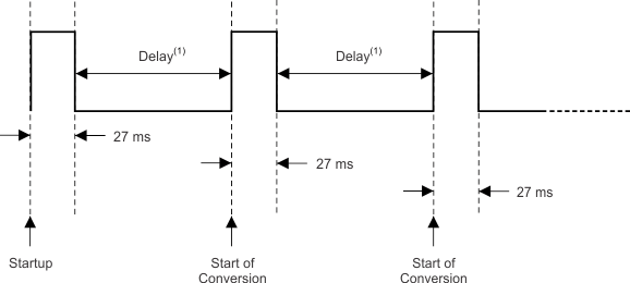
TMP108 ai_conv_bos663.gif
Delay is set by the CR1 and CR0 bits in the configuration register.
Figure 12. Conversion Start