ZHCSH87B September   2017  – February 2020 TMP461-SP

PRODUCTION DATA.  

  1. 特性
  2. 应用
    1.     简化框图
  3. 说明
  4. 修订历史记录
  5. Pin Configuration and Functions
    1.     Pin Functions
  6. Specifications
    1. 6.1 Absolute Maximum Ratings
    2. 6.2 ESD Ratings
    3. 6.3 Recommended Operating Conditions
    4. 6.4 Thermal Information
    5. 6.5 Electrical Characteristics
    6. 6.6 Two-Wire Timing Requirements
    7. 6.7 Typical Characteristics
  7. Detailed Description
    1. 7.1 Overview
    2. 7.2 Functional Block Diagram
    3. 7.3 Feature Description
      1. 7.3.1 Temperature Measurement Data
        1. 7.3.1.1 Standard Binary to Decimal Temperature Data Calculation Example
        2. 7.3.1.2 Standard Decimal to Binary Temperature Data Calculation Example
      2. 7.3.2 Series Resistance Cancellation
      3. 7.3.3 Differential Input Capacitance
      4. 7.3.4 Filtering
      5. 7.3.5 Sensor Fault
      6. 7.3.6 ALERT and THERM Functions
    4. 7.4 Device Functional Modes
      1. 7.4.1 Shutdown Mode (SD)
    5. 7.5 Programming
      1. 7.5.1 Serial Interface
        1. 7.5.1.1 Bus Overview
        2. 7.5.1.2 Bus Definitions
        3. 7.5.1.3 Serial Bus Address
        4. 7.5.1.4 Read and Write Operations
        5. 7.5.1.5 Timeout Function
        6. 7.5.1.6 High-Speed Mode
      2. 7.5.2 General-Call Reset
    6. 7.6 Register Map
      1. 7.6.1 Register Information
        1. 7.6.1.1  Pointer Register
        2. 7.6.1.2  Local and Remote Temperature Registers
        3. 7.6.1.3  Status Register
        4. 7.6.1.4  Configuration Register
        5. 7.6.1.5  Conversion Rate Register
        6. 7.6.1.6  One-Shot Start Register
        7. 7.6.1.7  Channel Enable Register
        8. 7.6.1.8  Consecutive ALERT Register
        9. 7.6.1.9  η-Factor Correction Register
        10. 7.6.1.10 Remote Temperature Offset Register
        11. 7.6.1.11 Manufacturer Identification Register
  8. Application and Implementation
    1. 8.1 Application Information
    2. 8.2 Typical Application
      1. 8.2.1 Design Requirements
      2. 8.2.2 Detailed Design Procedure
      3. 8.2.3 Application Curve
    3. 8.3 Radiation Environments
      1. 8.3.1 Single Event Latch-Up
      2. 8.3.2 Single Event Functional Interrupt
      3. 8.3.3 Single Event Upset
  9. Power Supply Recommendations
  10. 10Layout
    1. 10.1 Layout Guidelines
    2. 10.2 Layout Example
  11. 11器件和文档支持
    1. 11.1 接收文档更新通知
    2. 11.2 社区资源
    3. 11.3 商标
    4. 11.4 静电放电警告
    5. 11.5 Glossary
  12. 12机械、封装和可订购信息

封装选项

机械数据 (封装 | 引脚)
散热焊盘机械数据 (封装 | 引脚)
订购信息

ALERT and THERM Functions

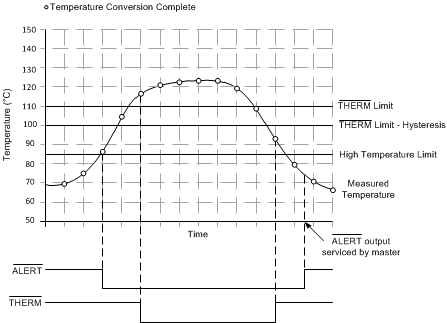
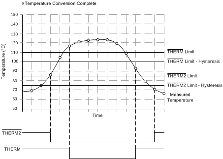
Operation of the ALERT (pin 7) and THERM (pin 4) interrupts is shown in Figure 13. Operation of the THERM (pin 4) and THERM2 (pin 7) interrupts is shown in Figure 14. The ALERT and THERM pin setting is determined by bit 5 of the configuration register.

The hysteresis value is stored in the THERM hysteresis register and applies to both the THERM and THERM2 interrupts. The value of the CONAL[2:0] bits in the consecutive ALERT register (see Table 5) determines the number of limit violations before the ALERT pin is tripped. The default value is 000b and corresponds to one violation, 001b programs two consecutive violations, 011b programs three consecutive violations, and 111b programs four consecutive violations. The CONAL[2:0] bits provide additional filtering for the ALERT pin state.
TMP461-SP ai_alertresp_slos877.gif
Figure 13. ALERT and THERM Interrupt Operation
TMP461-SP ai_thermresp_slos877.gif
Figure 14. THERM and THERM2 Interrupt Operation