ZHCSJR5 May   2019 TMUX1219

PRODUCTION DATA.  

  1. 特性
  2. 应用
  3. 说明
    1.     Device Images
      1.      应用示例
      2.      方框图
  4. 修订历史记录
  5. Pin Configuration and Functions
    1.     Pin Functions
  6. Specifications
    1. 6.1 Absolute Maximum Ratings
    2. 6.2 ESD Ratings
    3. 6.3 Recommended Operating Conditions
    4. 6.4 Thermal Information
    5. 6.5 Electrical Characteristics (VDD = 5 V ±10 %)
    6. 6.6 Electrical Characteristics (VDD = 3.3 V ±10 %)
    7. 6.7 Electrical Characteristics (VDD = 1.8 V ±10 %)
    8. 6.8 Electrical Characteristics (VDD = 1.2 V ±10 %)
    9. 6.9 Typical Characteristics
  7. Parameter Measurement Information
    1. 7.1 On-Resistance
    2. 7.2 Off-Leakage Current
    3. 7.3 On-Leakage Current
    4. 7.4 Transition Time
    5. 7.5 Break-Before-Make
    6. 7.6 Charge Injection
    7. 7.7 Off Isolation
    8. 7.8 Crosstalk
    9. 7.9 Bandwidth
  8. Detailed Description
    1. 8.1 Functional Block Diagram
    2. 8.2 Feature Description
      1. 8.2.1 Bidirectional Operation
      2. 8.2.2 Rail to Rail Operation
      3. 8.2.3 1.8 V Logic Compatible Inputs
      4. 8.2.4 Fail-Safe Logic
    3. 8.3 Device Functional Modes
    4. 8.4 Truth Tables
  9. Application and Implementation
    1. 9.1 Application Information
    2. 9.2 Typical Application
      1. 9.2.1 Switchable Operational Amplifier Gain Setting
        1. 9.2.1.1 Design Requirements
        2. 9.2.1.2 Detailed Design Procedure
        3. 9.2.1.3 Application Curve
      2. 9.2.2 Input Control for Power Amplifier
        1. 9.2.2.1 Design Requirements
        2. 9.2.2.2 Detailed Design Procedure
        3. 9.2.2.3 Application Curve
  10. 10Power Supply Recommendations
  11. 11Layout
    1. 11.1 Layout Guidelines
      1. 11.1.1 Layout Information
    2. 11.2 Layout Example
  12. 12器件和文档支持
    1. 12.1 文档支持
      1. 12.1.1 相关文档
    2. 12.2 接收文档更新通知
    3. 12.3 社区资源
    4. 12.4 商标
    5. 12.5 静电放电警告
    6. 12.6 Glossary
  13. 13机械、封装和可订购信息

封装选项

机械数据 (封装 | 引脚)
散热焊盘机械数据 (封装 | 引脚)
订购信息

Off Isolation

Off isolation is defined as the ratio of the signal at the drain pin (D) of the device when a signal is applied to the source pin (Sx) of an off-channel. Figure 13 shows the setup used to measure, and the equation used to calculate off isolation.
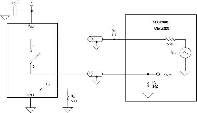
TMUX1219 Off_Isolation.gifFigure 13. Off Isolation Measurement Setup
Equation 1. TMUX1219 q_off_iso_sbas758.gif