ZHCSNC9C february 2021 – july 2023 TMUX7308F , TMUX7309F
PRODUCTION DATA
- 1
- 1 特性
- 2 应用
- 3 说明
- 4 Revision History
- 5 Device Comparison Table
- 6 Pin Configuration and Functions
-
7 Specifications
- 7.1 Absolute Maximum Ratings
- 7.2 ESD Ratings
- 7.3 Thermal Information
- 7.4 Recommended Operating Conditions
- 7.5 Electrical Characteristics (Global)
- 7.6 ±15 V Dual Supply: Electrical Characteristics
- 7.7 ±20 V Dual Supply: Electrical Characteristics
- 7.8 12 V Single Supply: Electrical Characteristics
- 7.9 36 V Single Supply: Electrical Characteristics
- 7.10 Typical Characteristics
-
8 Parameter Measurement Information
- 8.1 On-Resistance
- 8.2 Off-Leakage Current
- 8.3 On-Leakage Current
- 8.4 Input and Output Leakage Current Under Overvoltage Fault
- 8.5 Break-Before-Make Delay
- 8.6 Enable Delay Time
- 8.7 Transition Time
- 8.8 Fault Response Time
- 8.9 Fault Recovery Time
- 8.10 Charge Injection
- 8.11 Off Isolation
- 8.12 Crosstalk
- 8.13 Bandwidth
- 8.14 THD + Noise
- 9 Detailed Description
- 10Application and Implementation
- 11Device and Documentation Support
- 12Mechanical, Packaging, and Orderable Information
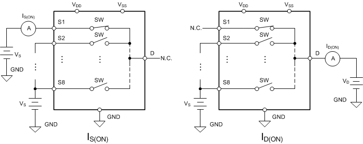
8.3 On-Leakage Current
Source on-leakage current (IS(ON)) and drain on-leakage current (ID(ON)) denote the channel leakage currents when the switch is in the on state. IS(ON) is measured with the drain floating, while ID(ON) is measured with the source floating. Figure 8-3 shows the circuit used for measuring the on-leakage currents.
 Figure 8-3 On-Leakage Measurement Setup