ZHCS891G April 2012 – December 2017 TPA3116D2 , TPA3118D2 , TPA3130D2
PRODUCTION DATA.
- 1 特性
- 2 应用
- 3 说明
- 4 修订历史记录
- 5 Pin Configuration and Functions
- 6 Specifications
-
7 Detailed Description
- 7.1 Overview
- 7.2 Functional Block Diagram
- 7.3
Feature Description
- 7.3.1 Gain Setting and Master and Slave
- 7.3.2 Input Impedance
- 7.3.3 Startup and Shutdown Operation
- 7.3.4 PLIMIT Operation
- 7.3.5 GVDD Supply
- 7.3.6 BSPx AND BSNx Capacitors
- 7.3.7 Differential Inputs
- 7.3.8 Device Protection System
- 7.3.9 DC Detect Protection
- 7.3.10 Short-Circuit Protection and Automatic Recovery Feature
- 7.3.11 Thermal Protection
- 7.3.12 Device Modulation Scheme
- 7.3.13 Efficiency: LC Filter Required with the Traditional Class-D Modulation Scheme
- 7.3.14 Ferrite Bead Filter Considerations
- 7.3.15 When to Use an Output Filter for EMI Suppression
- 7.3.16 AM Avoidance EMI Reduction
- 7.4 Device Functional Modes
- 8 Application and Implementation
- 9 Power Supply Recommendations
- 10Layout
- 11器件和文档支持
- 12机械、封装和可订购信息
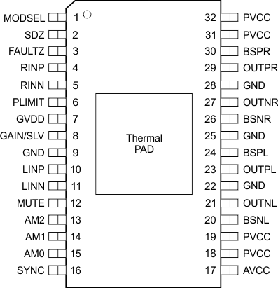
5 Pin Configuration and Functions
DAD Package
32-Pin HTSSOP With PowerPAD Up
TPA3116D2 Only, Top View

DAP Package
32-Pin HTSSOP With PowerPAD Down
Top View

Pin Functions
| PIN | TYPE(1) | DESCRIPTION | |
|---|---|---|---|
| NO. | NAME | ||
| 1 | MODSEL | I | Mode selection logic input (LOW = BD mode, HIGH = 1 SPW mode). TTL logic levels with compliance to AVCC. |
| 2 | SDZ | I | Shutdown logic input for audio amp (LOW = outputs Hi-Z, HIGH = outputs enabled). TTL logic levels with compliance to AVCC. |
| 3 | FAULTZ | DO | General fault reporting including Over-temp, DC Detect. Open drain. FAULTZ = High, normal operation FAULTZ = Low, fault condition |
| 4 | RINP | I | Positive audio input for right channel. Biased at 3 V. |
| 5 | RINN | I | Negative audio input for right channel. Biased at 3 V. |
| 6 | PLIMIT | I | Power limit level adjust. Connect a resistor divider from GVDD to GND to set power limit. Connect directly to GVDD for no power limit. |
| 7 | GVDD | PO | Internally generated gate voltage supply. Not to be used as a supply or connected to any component other than a 1 µF X7R ceramic decoupling capacitor and the PLIMIT and GAIN/SLV resistor dividers. |
| 8 | GAIN/SLV | I | Selects Gain and selects between Master and Slave mode depending on pin voltage divider. |
| 9 | GND | G | Ground |
| 10 | LINP | I | Positive audio input for left channel. Biased at 3 V. Connect to GND for PBTL mode. |
| 11 | LINN | I | Negative audio input for left channel. Biased at 3 V. Connect to GND for PBTL mode. |
| 12 | MUTE | I | Mute signal for fast disable/enable of outputs (HIGH = outputs Hi-Z, LOW = outputs enabled). TTL logic levels with compliance to AVCC. |
| 13 | AM2 | I | AM Avoidance Frequency Selection |
| 14 | AM1 | I | AM Avoidance Frequency Selection |
| 15 | AM0 | I | AM Avoidance Frequency Selection |
| 16 | SYNC | DIO | Clock input/output for synchronizing multiple class-D devices. Direction determined by GAIN/SLV terminal. |
| 17 | AVCC | P | Analog Supply |
| 18 | PVCC | P | Power supply |
| 19 | PVCC | P | Power supply |
| 20 | BSNL | BST | Boot strap for negative left channel output, connect to 220 nF X5R, or better ceramic cap to OUTNL |
| 21 | OUTNL | PO | Negative left channel output |
| 22 | GND | G | Ground |
| 23 | OUTPL | PO | Positive left channel output |
| 24 | BSPL | BST | Boot strap for positive left channel output, connect to 220 nF X5R, or better ceramic cap to OUTPL |
| 25 | GND | G | Ground |
| 26 | BSNR | BST | Boot strap for negative right channel output, connect to 220 nF X5R, or better ceramic cap to OUTNR |
| 27 | OUTNR | PO | Negative right channel output |
| 28 | GND | G | Ground |
| 29 | OUTPR | PO | Positive right channel output |
| 30 | BSPR | BST | Boot strap for positive right channel output, connect to 220 nF X5R or better ceramic cap to OUTPR |
| 31 | PVCC | P | Power supply |
| 32 | PVCC | P | Power supply |
| 33 | PowerPAD | G | Connect to GND for best system performance. If not connected to GND, leave floating. |
(1) TYPE: DO = Digital Output, I = Analog Input, G = General Ground, PO = Power Output, BST = Boot Strap.