ZHCS891G April 2012 – December 2017 TPA3116D2 , TPA3118D2 , TPA3130D2
PRODUCTION DATA.
- 1 特性
- 2 应用
- 3 说明
- 4 修订历史记录
- 5 Pin Configuration and Functions
- 6 Specifications
-
7 Detailed Description
- 7.1 Overview
- 7.2 Functional Block Diagram
- 7.3
Feature Description
- 7.3.1 Gain Setting and Master and Slave
- 7.3.2 Input Impedance
- 7.3.3 Startup and Shutdown Operation
- 7.3.4 PLIMIT Operation
- 7.3.5 GVDD Supply
- 7.3.6 BSPx AND BSNx Capacitors
- 7.3.7 Differential Inputs
- 7.3.8 Device Protection System
- 7.3.9 DC Detect Protection
- 7.3.10 Short-Circuit Protection and Automatic Recovery Feature
- 7.3.11 Thermal Protection
- 7.3.12 Device Modulation Scheme
- 7.3.13 Efficiency: LC Filter Required with the Traditional Class-D Modulation Scheme
- 7.3.14 Ferrite Bead Filter Considerations
- 7.3.15 When to Use an Output Filter for EMI Suppression
- 7.3.16 AM Avoidance EMI Reduction
- 7.4 Device Functional Modes
- 8 Application and Implementation
- 9 Power Supply Recommendations
- 10Layout
- 11器件和文档支持
- 12机械、封装和可订购信息
7.3.4 PLIMIT Operation
The TPA31xxD2 family has a built-in voltage limiter that can be used to limit the output voltage level below the supply rail, the amplifier simply operates as if it was powered by a lower supply voltage, and thereby limits the output power. Add a resistor divider from GVDD to ground to set the voltage at the PLIMIT pin. An external reference may also be used if tighter tolerance is required. Add a 1 µF capacitor from pin PLIMIT to ground to ensure stability. It is recommended to connect PLIMIT to GVDD when using 1SPW-modulation mode.
 Figure 29. Power Limit Example
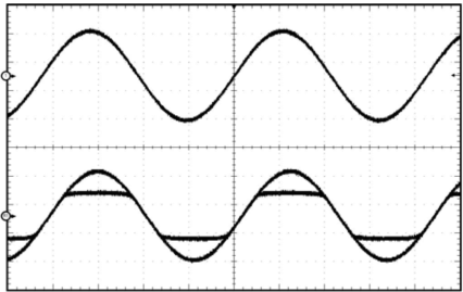
The PLIMIT circuit sets a limit on the output peak-to-peak voltage. The limiting is done by limiting the duty cycle to a fixed maximum value. This limit can be thought of as a "virtual" voltage rail which is lower than the supply connected to PVCC. This "virtual" rail is approximately 4 times the voltage at the PLIMIT pin. This output voltage can be used to calculate the maximum output power for a given maximum input voltage and speaker impedance.

where
- POUT (10% THD) = 1.25 × POUT (unclipped)
- RL is the load resistance.
- RS is the total series resistance including RDS(on), and output filter resistance.
- VP is the peak amplitude
- VP = 4 × PLIMIT voltage if PLIMIT < 4 × VP
Table 3. Power Limit Example
| PVCC (V) | PLIMIT VOLTAGE (V)(1) | R to GND | R to GVDD | OUTPUT VOLTAGE (Vrms) |
|---|---|---|---|---|
| 24 V | GVDD | Open | Short | 17.9 |
| 24 V | 3.3 | 45 kΩ | 51 kΩ | 12.67 |
| 24 V | 2.25 | 24 kΩ | 51 kΩ | 9 |
| 12 V | GVDD | Short | Open | 10.33 |
| 12 V | 2.25 | 24 kΩ | 51 kΩ | 9 |
| 12 V | 1.5 | 18 kΩ | 68 kΩ | 6.3 |